Ac waveforms – Rainbow Electronics AT45DB021D User Manual
Page 32
32
3638K–DFLASH–11/2012
AT45DB021D
Figure 16-2. Output Test Load
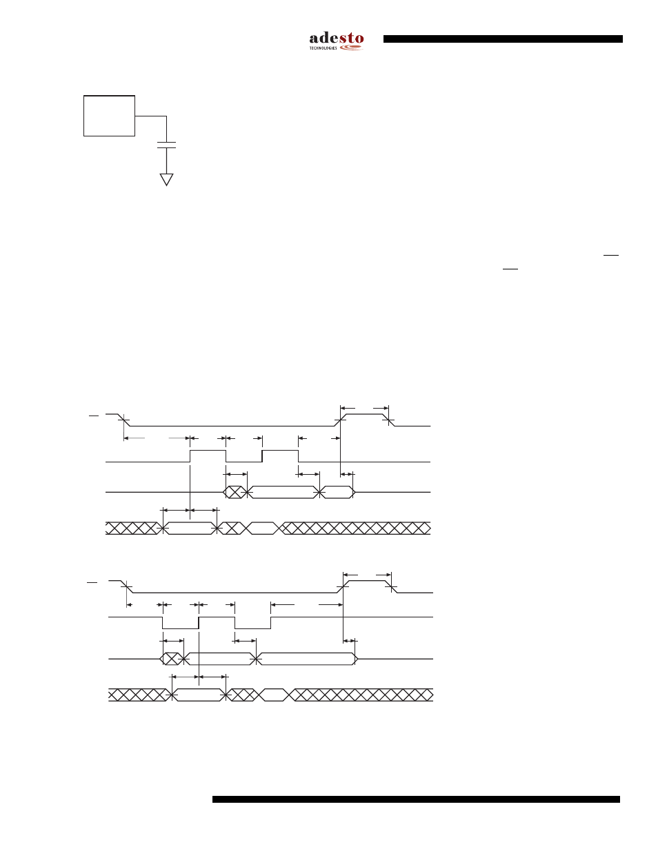
17.
AC Waveforms
Six different timing waveforms are shown on
. Waveform 1 shows the SCK signal being low when CS
makes a high-to-low transition, and waveform 2 shows the SCK signal being high when CS makes a high-to-low
transition. In both cases, output SO becomes valid while the SCK signal is still low (SCK low time is specified as
t
WL
). Timing waveforms 1 and 2 conform to RapidS serial interface but for frequencies up to 66MHz. Waveforms 1
and 2 are compatible with SPI Mode 0 and SPI Mode 3, respectively.
Waveform 3 and waveform 4 illustrate general timing diagram for RapidS serial interface. These are similar to
waveform 1 and waveform 2, except that output SO is not restricted to become valid during the t
WL
period. These
timing waveforms are valid over the full frequency range (maximum frequency = 66MHz) of the RapidS serial case.
Figure 17-1. Waveform 1 – SPI Mode 0 Compatible (for Frequencies up to 66MHz)
Figure 17-2. Waveform 2 – SPI Mode 3 Compatible (for Frequencies up to 66MHz)
DEVICE
UNDER
TEST
30pF
CS
SCK
SI
SO
t
CSS
VALID IN
t
H
t
SU
t
WH
t
WL
t
CSH
t
CS
t
V
HIGH IMPEDANCE
VALID OUT
t
HO
t
DIS
HIGH IMPEDANCE
CS
SCK
SO
t
CSS
VALID IN
t
H
t
SU
t
WL
t
WH
t
CSH
t
CS
t
V
HIGH Z
VALID OUT
t
HO
t
DIS
HIGH IMPEDANCE
SI