Ata6824 [preliminary, Electrical characteristics (continued) – Rainbow Electronics ATA6824 User Manual
Page 17
17
4931C–AUTO–09/06
ATA6824 [Preliminary]
3.17
Internal pull-up resistor at
pin /RESET
5
R
PURES
5
10 15
k
Ω
D
4
High Voltage Serial Interface
4.1
Low-level output current
Normal mode;
V
LIN
= 0V, V
RX
= 0.4V
13
IL
RX
4
mA
D
4.2
High-level output current
Normal mode;
V
LIN
= V
BAT
V
RX
= V
CC
– 0.4V
13
IH
RX
4
mA
D
4.3
Driver recessive output
voltage
V
TXD
= 0V; I
LIN
= 0 mA
8
V
BUSrec
0.9
×
VBAT
V
4.4
Driver dominant voltage
V
BUSdom_DRV_LoSUP
V
VAT
= 7.3V
R
load
= 500
Ω
8
V
_LoSUP
1.2
V
4.5
Driver dominant voltage
V
BUSdom_DRV_HiSUP
V
VAT
= 18V
R
load
= 500
Ω
8
V
_HiSUP
2
V
4.6
Driver dominant voltage
V
BUSdom_DRV_LoSUP
V
VAT
= 7.3V
R
load
= 1000
Ω
8
V
_LoSUP_1k
0.6
V
4.7
Driver dominant voltage
V
BUSdom_DRV_HiSUP
V
VAT
= 18V
R
load
= 1000
Ω
8
V
_HiSUP_1k_
0.8
V
4.8
Pull up resistor to VS
The serial diode is
mandatory
8
R
LIN
20
30
60
k
Ω
D
4.9
Current limitation
V
BUS
= V
BAT_max
8
I
BUS_LIM
50
200
mA
4.10
Input leakage current at
the receiver including
pull-up resistor as
specified
Input leakage current
driver off
V
BUS
= 0V
V
BAT
= 12V
8
I
BUS_PAS_dom
–1
mA
4.11
Leakage current SIO
recessive
Driver off
8V < V
BAT
< 18V
8V < V
BUS
< 18V
V
BUS
≥
V
BAT
8
I
BUS_PAS_rec
30
µA
4.12
Leakage current at
ground loss
Control unit disconnected
from ground
Loss of local ground must
not affect communication
in the residual network
GND
Device
= VS
V
BAT
=12V
0V < V
BUS
< 18V
8
I
BUS_NO_gnd
–1
1
mA
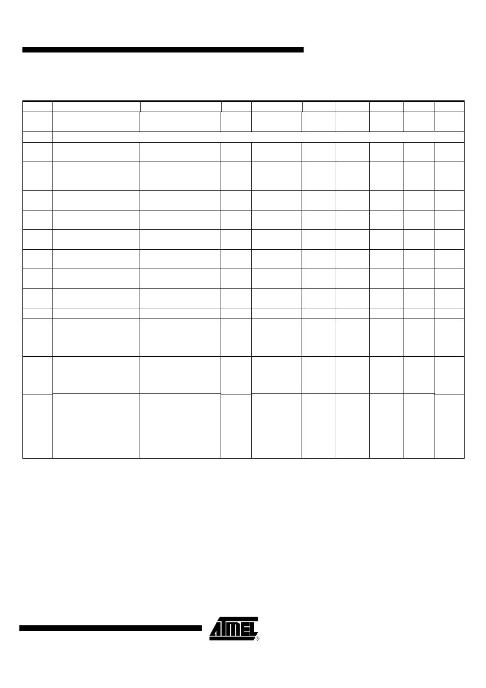
10. Electrical Characteristics (Continued)
All parameters given are valid for 7V
≤
VBAT
≤
18V and for –40°C
≤ ϑ
ambient
≤
150°C unless stated otherwise.
No.
Parameters
Test Conditions
Pin
Symbol
Min
Typ
Max
Unit
Type*
* Type: A = 100% tested, B = 100% correlation tested, C = Characterized on samples, D = Design parameter
Notes:
1. EN, DIR, PWM = high
2. The use of X7R material is recommended
3. For higher values, stability at zero load is not guaranteed
4. Tested during qualification only
5. Value depends on T
OSC
; function tested with digital test pattern
6. Tested during characterization only
7. Supplied by charge pump
8. See section
“Cross Conduction Time”
9. Voltage between source-drain of external switching transistors in active case
10. The short-circuit message will never be generated for switch-on time < t
sc