Ata6824 [preliminary, Absolute maximum ratings – Rainbow Electronics ATA6824 User Manual
Page 13
13
4931C–AUTO–09/06
ATA6824 [Preliminary]
6.
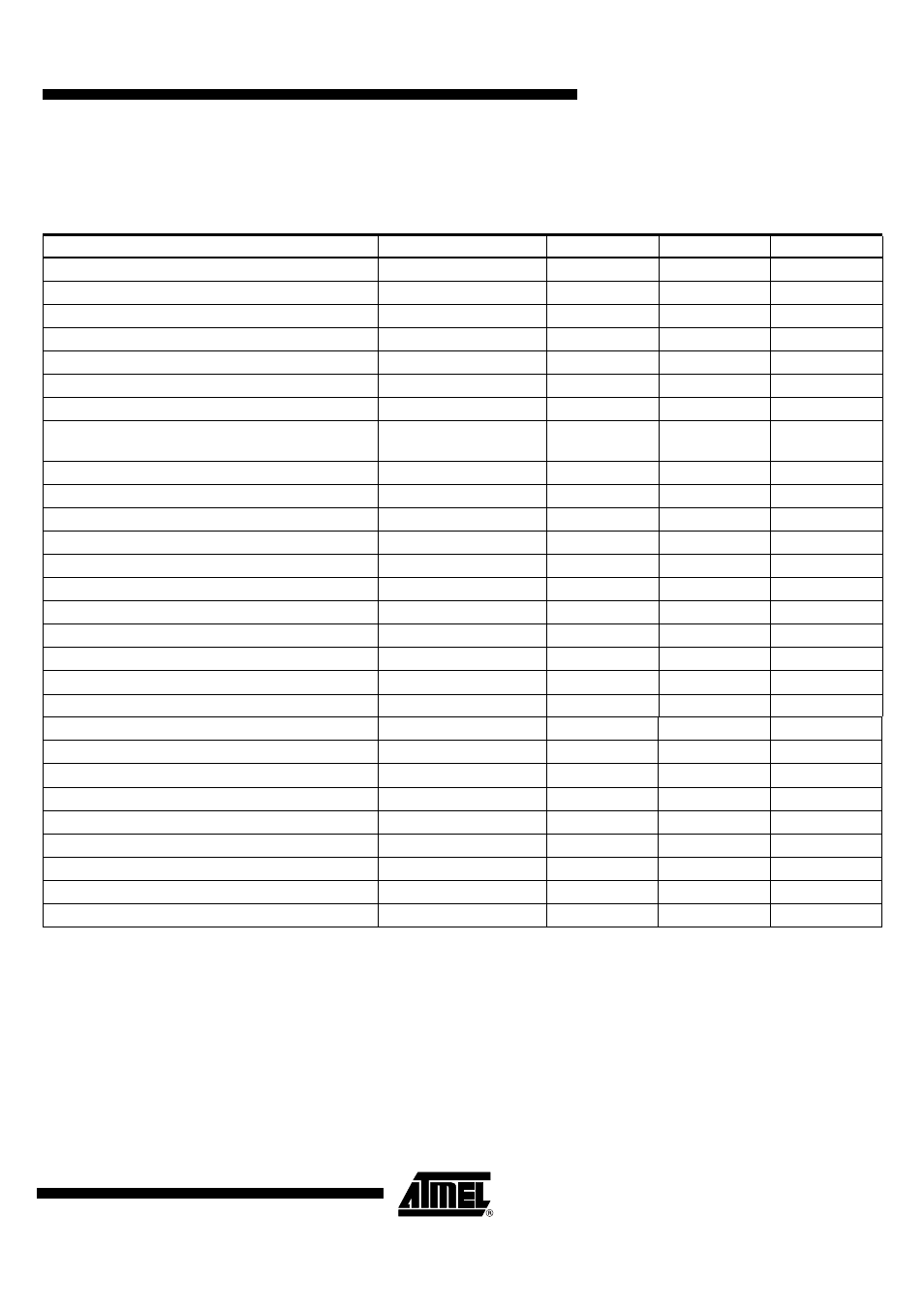
Absolute Maximum Ratings
Stresses beyond those listed under “Absolute Maximum Ratings” may cause permanent damage to the device. This is a stress rating
only and functional operation of the device at these or any other conditions beyond those indicated in the operational sections of this
specification is not implied. Exposure to absolute maximum rating conditions for extended periods may affect device reliability.
Pin Description
Pin Name
Min
Max
Unit
Ground
GND
0
0
V
Power ground
PGND
–0.3
+0.3
V
Reverse protected battery voltage
VBAT
–0.3
+40
V
Reverse protected battery voltage
PBAT
–0.3
+40
V
Digital output
/RESET
–0.3
V
VCC
+ 0.3
V
Digital output
DG1, DG2, DG3
–0.3
V
VCC
+ 0.3
V
4.9V output, external blocking capacitor
VINT
–0.3
+5.5
V
Cross conduction time capacitor/resistor
combination
CC
–0.3
V
VINT
+ 0.3
V
Digital input coming from microcontroller
WD
–0.3
V
VINT
+ 0.3
V
Watchdog timing resistor
RWD
–0.3
V
VCC
+ 0.3
V
Digital input direction control
DIR
–0.3
V
VCC
+ 0.3
V
Digital input PWM control + Test mode
PWM
–0.3
V
VCC
+ 0.3
V
5V regulator output
VCC
–0.3
+5.5
V
Digital input
VMODE
–0.3
V
VINT
+ 0.3
V
12V output, external blocking capacitor
VG
–0.3
+16
V
Digital output
RX
–0.3
V
VCC
+ 0.3
V
Digital input
TX
–0.3
V
VCC
+ 0.3
V
LIN data pin
SIO
–27
(1)
V
VBAT
+ 2
V
Source external high-side NMOS
S1, S2
–2
+30
V
Gates external low-side NMOS
L1, L2
V
PGND
– 0.3
V
VG
+ 0.3
V
Gates of external high-side NMOS
H1, H2
V
S
– 1
V
S
+ 16
V
Charge pump
CPLO
–0.3
V
PBAT
+ 0.3
V
Charge pump
CPHI
–0.3
V
VRES
+ 0.3
V
Charge pump output
VRES
–0.3
+30
V
Switched VBAT
VBATSW
–0.3
V
VBAT
+ 0.3
V
Power dissipation
P
tot
1.4
(2)
W
Storage temperature
ϑ
STORE
–55
+200
°C
Soldering temperature (10s)
ϑ
SOLDERING
240
°C
Notes:
1. For V
VBAT
≤
13.5V
2. May be additionally limited by external thermal resistance