Ata6824 [preliminary, Electrical characteristics – Rainbow Electronics ATA6824 User Manual
Page 15
15
4931C–AUTO–09/06
ATA6824 [Preliminary]
10. Electrical Characteristics
All parameters given are valid for 7V
≤
VBAT
≤
18V and for –40°C
≤ ϑ
ambient
≤
150°C unless stated otherwise.
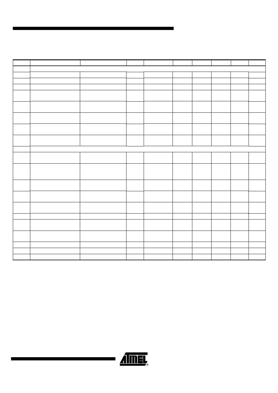
No.
Parameters
Test Conditions
Pin
Symbol
Min
Typ
Max
Unit
Type*
1
Power Supply and Supervisor Functions
1.1
Current consumption V
BAT
V
VBAT
= 13.5V
(1)
25, 30
I
VBAT1
7
mA
A
1.2
Internal power supply
2
V
INT
4.8
4.94
5.1
V
A
1.3
Band gap voltage
V
BG
1.235
V
A
1.4
Overvoltage threshold
V
BAT
30
V
THOV
19.8
22.3
V
A
1.5
Overvoltage threshold
hysteresis V
BAT
Measured during
qualification only
30
V
TOVhys
1
1.5
V
A
1.6
Undervoltage threshold
V
BAT
30
V
THUV
6.5
7
V
A
1.7
Undervoltage threshold
hysteresis V
BAT
Measured during
qualification only
30
V
TUVhys
0.2
0.4
V
A
1.8
On resistance of V
BAT
switch
V
VBAT
= 13.5V
31
R
ON_VBATSW
100
Ω
A
2
5V/3.3V Regulator
2.1
Regulated output voltage
9V < V
VBAT
< 40V,
I
load
= 0 mA to 100 mA
29
V
CC1
4.85
(3.2)
5.15
(3.4)
V
A
2.1a
Regulated output voltage
9V < V
VBAT
< 40V,
I
load
= 0 mA to 80 mA,
T
a
> 125°C
29
V
CC1
4.85
(3.2)
5.15
(3.4)
V
A
2.2
Regulated output voltage
6V < V
VBAT
≤
9V
I
load
= 0 mA to 100 mA
29
V
CC2
4.75
(3.2)
5.25
(3.4)
V
A
2.3
Line regulation
I
load
= 0 mA to 100 mA
29
DC line
regulation
<1
50
mV
A
2.4
Load regulation
I
load
= 0 mA to 100 mA
29
DC load
regulation
<10
50
mV
A
2.5
Output current limitation
V
VBAT
> 6V
29
I
OS1
100
300
mA
C
2.6
Serial inductance to C
VCC
including PCB
29
ESL
1
20
nH
D
2.7
Serial resistance to C
VCC
including PCB
29
ESR
0
0.5
Ω
D
2.8
Blocking cap at VCC
(2), (3)
29
C
VCC
1.5
3.0
µF
D
2.9
HIGH threshold VMODE
1
VMODE H
4.0
V
A
2.10
LOW threshold VMODE
1
VMODE L
0.7
V
A
* Type: A = 100% tested, B = 100% correlation tested, C = Characterized on samples, D = Design parameter
Notes:
1. EN, DIR, PWM = high
2. The use of X7R material is recommended
3. For higher values, stability at zero load is not guaranteed
4. Tested during qualification only
5. Value depends on T
OSC
; function tested with digital test pattern
6. Tested during characterization only
7. Supplied by charge pump
8. See section
9. Voltage between source-drain of external switching transistors in active case
10. The short-circuit message will never be generated for switch-on time < t
sc