6 program and erase characteristics, 7 power-up conditions, 8 input test waveforms and measurement levels – Rainbow Electronics AT25DQ321 User Manual
Page 56: 9 output test load
56
AT25DQ321 [DATASHEET]
8718D–DFLASH–12/2012
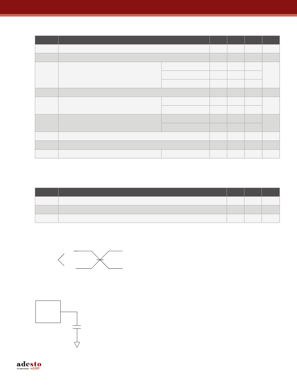
13.6 Program and Erase Characteristics
Notes: 1. Maximum values indicate worst-case performance after 100,000 erase/program cycles.
2. Not 100% tested. (Value guaranteed by design and characterization)
13.7 Power-up Conditions
13.8 Input Test Waveforms and Measurement Levels
13.9 Output Test Load
Symbol
Parameter
Min
Typ
Max
Units
t
PP
Page Program Time (256-bytes)
1.5
3.0
ms
t
BP
Byte Program Time
7
μs
t
BLKE
Block Erase Time
4KB
50
200
ms
32KB
250
600
64KB
400
950
t
CHPE
Chip Erase Time
25
40
sec
t
SUSP
Suspend Time
Program
10
20
μs
Erase
25
40
t
RES
Resume Time
Program
10
20
μs
Erase
12
20
t
OTPP
OTP Security Register Program Time
200
500
μs
t
WRSR
Write Status Register Time
200
ns
t
WRCR
Write Configuration Register Time
15
35
ms
Symbol
Parameter
Min
Max
Units
t
VCSL
Minimum V
CC
to Chip Select Low Time
70
μs
t
PUW
Power-Up Device Delay Before Program or Erase Allowed
10
ms
V
POR
Power-On Reset Voltage
1.5
2.5
V
AC
Driving
Levels
AC
Measurement
Level
0.1V
CC
V
CC
/2
0.9V
CC
t
R
, t
F
< 2ns (10% to 90%)
Device
Under
Test
15pF (Frequencies above 70MHz)
or
30pF