1 qe bit, And hold is i/o – Rainbow Electronics AT25DQ321 User Manual
Page 46
46
AT25DQ321 [DATASHEET]
8718D–DFLASH–12/2012
11.4.1 QE Bit
The QE bit is used to control whether the Quad-Input Byte/Page Program and Quad-Output Read Array commands are
enabled or disabled. When the QE bit is in the Logical 1 state, the Quad-Input Byte/Page Program and Quad-Output
Read Array commands are enabled and will be recognized by the device. In addition, the WP and HOLD functions are
disabled and the WP and HOLD pins themselves operate as a bidirectional input/output pins (WP is I/O
2
and HOLD
is I/O
3
).
When the QE bit is in the Logical 0 state, the Quad-Input Byte/Page Program and Quad-Output Read Array commands
are disabled and will not be recognized by the device as valid commands and the WP and HOLD pins function as normal
control pins. The WP and HOLD pins should be externally pulled-high to avoid erroneous or unwanted device operation.
The Reset command has no effect on the QE bit. The QE bit defaults to the Logical 0 state when devices are initially
shipped from Adesto.
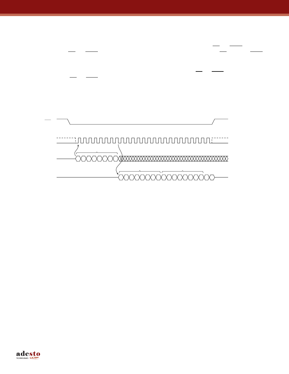
Figure 11-4. Read Configuration Register
SO
SI
SCK
CS
MSB
2
3
1
0
0
0
1
1
1
1
1
1
6
7
5
4
10 11
9
8
12
21 22
17
20
19
18
15 16
13 14
23 24
Opcode
MSB
MSB
X
X
X
X
X
X
D
X
X
D
MSB
X
X
X
X
X
X
X
D
Configuration
Register Out
Configuration
Register Out
High-impedance