Rainbow Electronics AT25DQ321 User Manual
Page 4
4
AT25DQ321 [DATASHEET]
8718D–DFLASH–12/2012
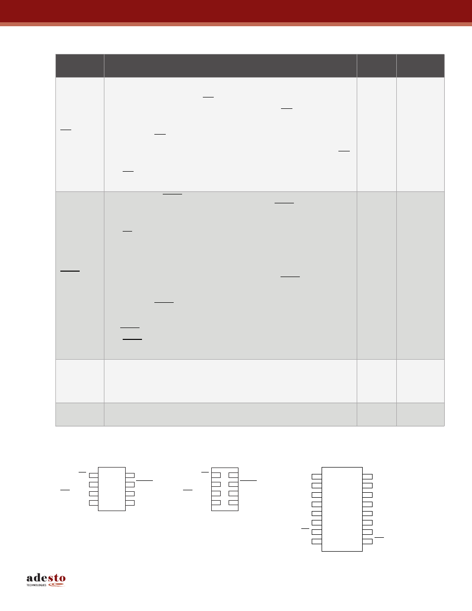
Figure 2-1. Pin Configurations
WP (I/O
2
)
Write Protect (I/O
2
): The WP# pin controls the hardware locking feature of the
device.
See “Protection Commands and Features” on page 24
for more details
on protection features and the WP pin.
With the Quad-Input Byte/Page Program command, the WP pin becomes an
input pin (I/O
2
) and, along with other pins, allows four bits (on I/O
3-0
) of data to
be clocked in on every rising edge of SCK. With the Quad-Output Read Array
command, the WP pin becomes an output pin (I/O
2
) and, when used with other
pins, allows four bits (on I/O
3-0
) of data to be clocked out on every falling edge of
SCK. The QE bit in the Configuration Register must be set in order for the WP
pin to be used as an I/O data pin.
The WP pin must be driven at all times or pulled-high using an external pull-up
resistor.
Low
Input/Output
HOLD (I/O
3
)
Hold (I/O
3
): The HOLD pin is used to temporarily pause serial communication
without deselecting or resetting the device. While the HOLD pin is asserted,
transitions on the SCK pin and data on the SI pin will be ignored and the SO pin
will be in a high-impedance state.
The CS pin must be asserted and the SCK pin must be in the low state in order
for a Hold condition to start. A Hold condition pauses serial communication only
and does not have an affect on internally self-timed operations such as a
program or erase cycle.
for additional details on the Hold
operation.
With the Quad-Input Byte/Page Program command, the HOLD pin becomes an
input pin (I/O
3
) and, along with other pins, allows four bits (on I/O
3-0
) of data to
be clocked in on every rising edge of SCK. With the Quad-Output Read Array
command, the HOLD pin becomes an output pin (I/O
3
) and, when used with
other pins, allows four bits (on I/O
3-0
) of data to be clocked out on every falling
edge of SCK. The QE bit in the Configuration Register must be set in order for
the HOLD pin to be used as an I/O data pin.
The HOLD pin must be driven at all times or pulled-high using an external
pull-up resistor.
Low
Input/Output
V
CC
Device Power Supply: The V
CC
pin is used to supply the source voltage to the
device.
Operations at invalid V
CC
voltages may produce spurious results and should not
be attempted.
-
Power
GND
Ground: The ground reference for the power supply. GND should be
connected to the system ground.
-
Power
Table 2-1.
Pin Descriptions (Continued)
Symbol
Name and Function
Asserted
State
Type
4
3
2
1
5
6
7
8
8-pad UDFN
1
2
3
4
8
7
6
5
8-lead SOIC
CS
SO (I/O
1
)
WP (I/O
2
)
GND
CS
SO (I/O
1
)
WP (I/O
2
)
GND
V
CC
HOLD (I/O
3
)
SCK
SI (I/O
0
)
16-lead SOIC
V
CC
HOLD (I/O
3
)
SCK
SI (I/O
0
)
1
2
3
4
5
6
7
8
16
15
14
13
12
11
10
9
NC
V
CC
NC
NC
NC
NC
CS
SO
SCK
SI
NC
NC
NC
NC
GND
WP