Write operations, Buffer write – Rainbow Electronics AT45DB011B User Manual
Page 16
16
AT45DB011B
1984E–DFLSH–10/02
Write
Operations
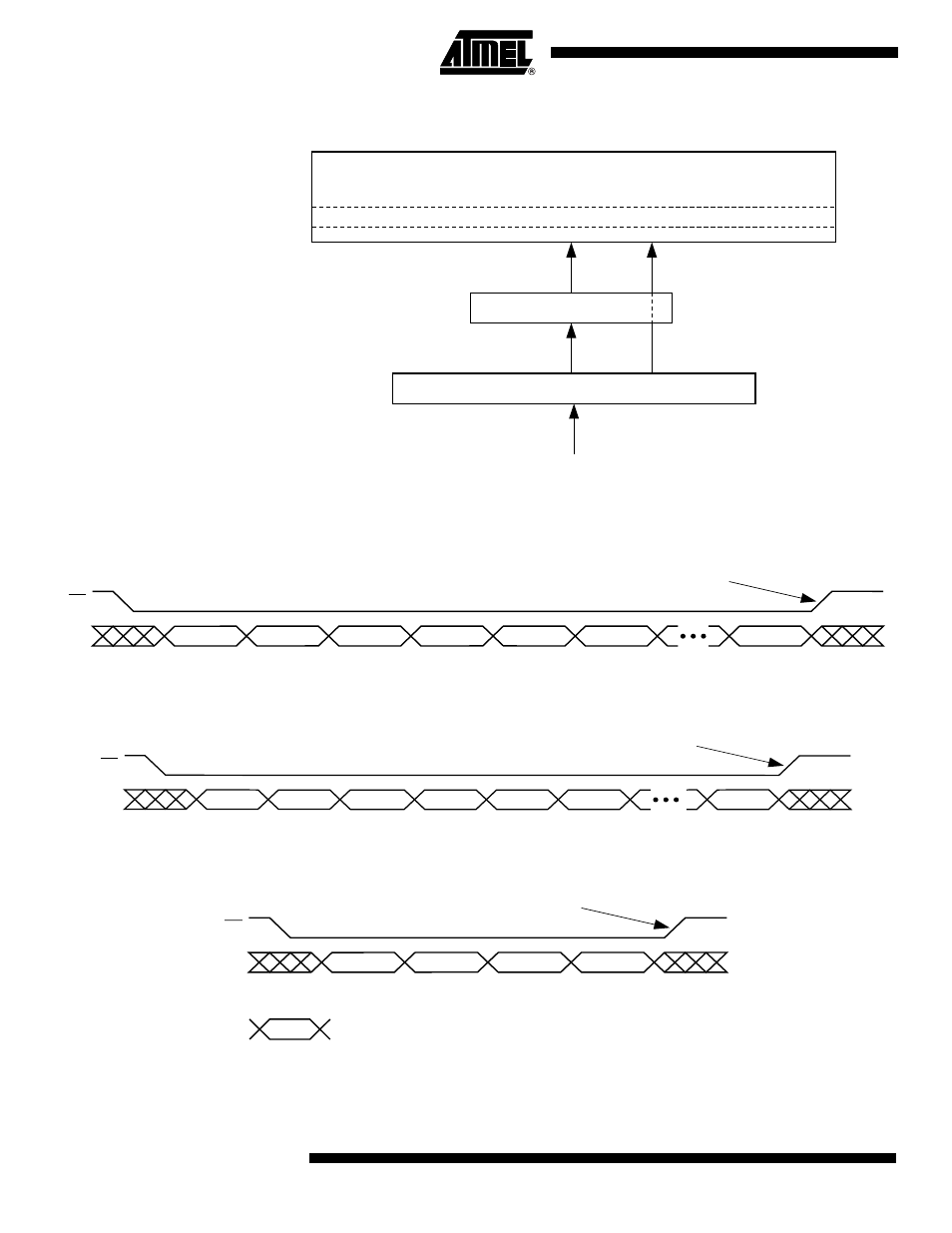
The following block diagram and waveforms illustrate the various write sequences available.
Main Memory Page Program through Buffer
Buffer Write
Buffer to Main Memory Page Program (Data from Buffer Programmed into Flash Page)
FLASH MEMORY ARRAY
PAGE (264 BYTES)
BUFFER (264 BYTES)
I/O INTERFACE
SI
BUFFER TO
MAIN MEMORY
PAGE PROGRAM
MAIN MEMORY PAGE
PROGRAM THROUGH
BUFFER
BUFFER
WRITE
SI
CMD
n
n+1
Last Byte
· Completes writing into buffer
· Starts self-timed erase/program operation
CS
r ···r , PA8-7
PA6-0, BFA8
BFA7-0
SI
CMD
X
X···X, BFA8
BFA7-0
n
n+1
Last Byte
· Completes writing into buffer
CS
SI
CMD
PA6-0, X
X
CS
Starts self-timed erase/program operation
r ···r , PA8-7
Each transition represents
8 bits and 8 clock cycles
n = 1st byte written
n+1 = 2nd byte written
- W27E010 (14 pages)
- W27L520 (16 pages)
- W29EE512 (21 pages)
- W27E512 (16 pages)
- W24100 (11 pages)
- W27E040 (15 pages)
- W25Q32 (60 pages)
- W49L102 (21 pages)
- W29C040 (20 pages)
- W29EE011 (20 pages)
- W49F020 (21 pages)
- W2465 (10 pages)
- W24256 (10 pages)
- W982516CH (43 pages)
- MAX16014 (12 pages)
- W24512A (10 pages)
- W27E020 (14 pages)
- W29C020C (21 pages)
- W25X64 (47 pages)
- W24257 (11 pages)
- W24L257 (10 pages)
- W9864G2GH (48 pages)
- W24L11 (11 pages)
- W27L010 (14 pages)
- W27E520 (16 pages)
- W27LE520 (16 pages)
- W9825G6CH (43 pages)
- W49F002U (23 pages)
- W9864G6GB (47 pages)
- AT45DB642 (71 pages)
- AT45DB642 (37 pages)
- AT45DB161D (51 pages)
- AT27LV040A (12 pages)
- AT29LV010A (15 pages)
- HT24LC08 (11 pages)
- AT29C257 (12 pages)
- AT45DB161B (32 pages)
- AT27C1024 (12 pages)
- AT28BV256 (12 pages)
- AT28C040 (12 pages)
- DS1258Y_AB (9 pages)
- AT28BV64B (12 pages)
- AT27C512R (12 pages)
- DS1220AB_AD (9 pages)