Input test waveforms and measurement levels, Output test load, Ac waveforms – Rainbow Electronics AT45DB011B User Manual
Page 14: Output test load ac waveforms
14
AT45DB011B
1984E–DFLSH–10/02
Input Test Waveforms and Measurement Levels
t
R
, t
F
< 3 ns (10% to 90%)
Output Test Load
AC Waveforms
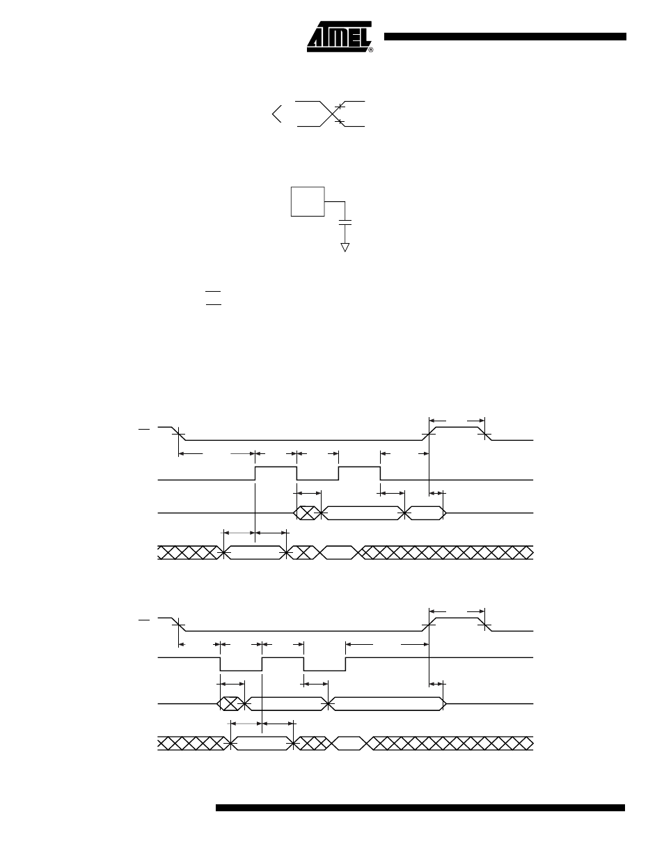
Two different timing diagrams are shown below. Waveform 1 shows the SCK signal being low
when CS makes a high-to-low transition, and Waveform 2 shows the SCK signal being high
when CS makes a high-to-low transition. Both waveforms show valid timing diagrams. The
setup and hold times for the SI signal are referenced to the low-to-high transition on the SCK
signal.
Waveform 1 shows timing that is also compatible with SPI Mode 0, and Waveform 2 shows
timing that is compatible with SPI Mode 3.
Waveform 1 – Inactive Clock Polarity Low and SPI Mode 0
Waveform 2 – Inactive Clock Polarity High and SPI Mode 3
AC
DRIVING
LEVELS
AC
MEASUREMENT
LEVEL
0.45V
2.0
0.8
2.4V
DEVICE
UNDER
TEST
30 pF
CS
SCK
SI
SO
t
CSS
VALID IN
t
H
t
SU
t
WH
t
WL
t
CSH
t
CS
t
V
HIGH IMPEDANCE
VALID OUT
t
HO
t
DIS
HIGH IMPEDANCE
CS
SCK
SI
SO
t
CSS
VALID IN
t
H
t
SU
t
WL
t
WH
t
CSH
t
CS
t
V
HIGH Z
VALID OUT
t
HO
t
DIS
HIGH IMPEDANCE