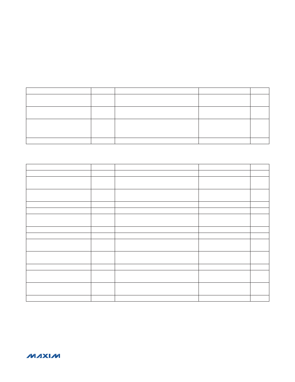
Electrical characteristics: 2-wire interface, Electrical characteristics (2-wire interface), Electrical characteristics (continued) – Rainbow Electronics MAX17047 User Manual
Page 3
����������������������������������������������������������������� Maxim Integrated Products 3
MAX17047
ModelGauge m3 Fuel Gauge
Note 1: Specifications are 100% tested at T
A
= +25°C. Limits over the operating range are guaranteed by design and
characterization.
Note 2: All voltages are referenced to CSP.
Note 3: Timing must be fast enough to prevent the device from entering shutdown mode due to bus low for a period > 45s minimum.
Note 4: f
SCL
must meet the minimum clock low time plus the rise/fall times.
Note 5: The maximum t
HD:DAT
has only to be met if the device does not stretch the low period (t
LOW
) of the SCL signal.
Note 6: This device internally provides a hold time of at least 100ns for the SDA signal (referred to the minimum VIH of the SCL
signal) to bridge the undefined region of the falling edge of SCL.
Note 7: Filters on SDA and SCL suppress noise spikes at the input buffers and delay the sampling instant.
Note 8: C
B
—total capacitance of one bus line in pF.
ELECTRICAL CHARACTERISTICS (2-WIRE INTERFACE)
(2.5V P V
BATT
P 4.5V, T
A
= -20NC to +70NC.) (Note 1)
ELECTRICAL CHARACTERISTICS (continued)
(V
BATT
= 2.5V to 4.5V, T
A
= -20NC to +70NC, unless otherwise noted. Typical values are at T
A
= +25NC.) (Note 1)
PARAMETER
SYMBOL
CONDITIONS
MIN
TYP
MAX
UNITS
Battery-Removal Detection
Threshold—V
AIN
Rising
V
DETR
V
THRM
- V
AIN
40
125
200
mV
Battery-Removal Detection
Threshold—V
AIN
Falling
V
DETF
V
THRM
- V
AIN
70
150
230
mV
Battery-Removal Detection
Comparator Delay
t
TOFF
V
AIN
step from 70% to 100% of V
THRM
to
ALRT falling; Alrtp = logic 0;
EnAIN = logic 1; FTHRM = logic 1
100
F
s
External AIN Capacitance
R
THM
= 10kI NTC
100
nF
PARAMETER
SYMBOL
CONDITIONS
MIN
TYP
MAX
UNITS
SCL Clock Frequency
f
SCL
(Note 3)
0
400
kHz
Bus Free Time Between a STOP
and START Condition
t
BUF
1.3
F
s
Hold Time (Repeated)
START Condition
t
HD:STA
(Note 4)
0.6
F
s
Low Period of SCL Clock
t
LOW
1.3
F
s
High Period of SCL Clock
t
HIGH
0.6
F
s
Setup Time for a Repeated
START Condition
t
SU:STA
0.6
F
s
Data Hold Time
t
HD:DAT
(Notes 5, 6)
0
0.9
F
s
Data Setup Time
t
SU:DAT
(Note 5)
100
ns
Rise Time of Both SDA and SCL
Signals
t
R
20 +
0.1C
B
300
ns
Fall Time of Both SDA and SCL
Signals
t
F
20 +
0.1C
B
300
ns
Setup Time for STOP Condition
t
SU:STO
0.6
F
s
Spike Pulse Widths
Suppressed by Input Filter
t
SP
(Note 7)
0
50
ns
Capacitive Load for Each Bus
Line
C
B
(Note 8)
400
pF
SCL, SDA Input Capacitance
C
BIN
60
pF