Rc1180-mbus – Rainbow Electronics RC1180-MBUS User Manual
Page 21
RC1180-MBUS
2008 Radiocrafts AS
RC1180-MBUS Data Sheet (rev. 1.0)
Page 21 of 28
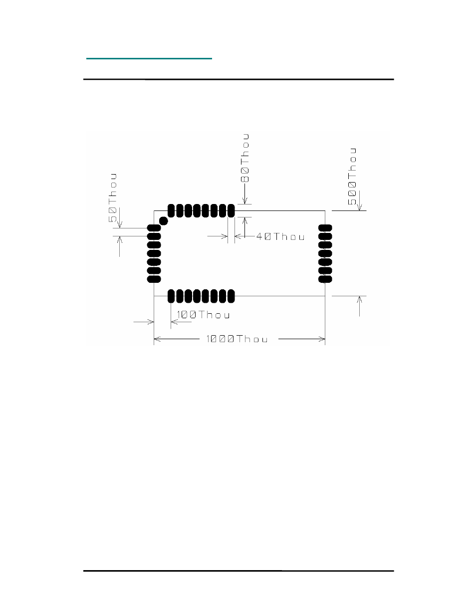
PCB Layout Recommendations
The recommended layout pads for the module are shown in the figure below. All dimensions
are in thousands of an inch (mil). The circle in upper left corner is an orientation mark only,
and should not be a part of the copper pattern.
A PCB with two or more layers and with a solid ground plane in one of the inner- or bottom
layer(s) is recommended. All GND-pins of the module shall be connected to this ground plane
with vias with shortest possible routing, one via per GND-pin.
On the back side of the module there are several test pads. These test pads shall not be
connected, and the area underneath the module should be covered with solder resist. If any
routing or vias is required under the module, the routing and vias must be covered with solder
resist to prevent short circuiting of the test pads. It is recommended that vias are tented.
Reserved pins should be soldered to the pads but the pads must be left floating.