Rainbow Electronics MAX5971B User Manual
Page 24
24 _____________________________________________________________________________________
MAX5971B
Single-Port, 40W, IEEE 802.3af/at,
PSE Controller with I
2
C
Slave Address
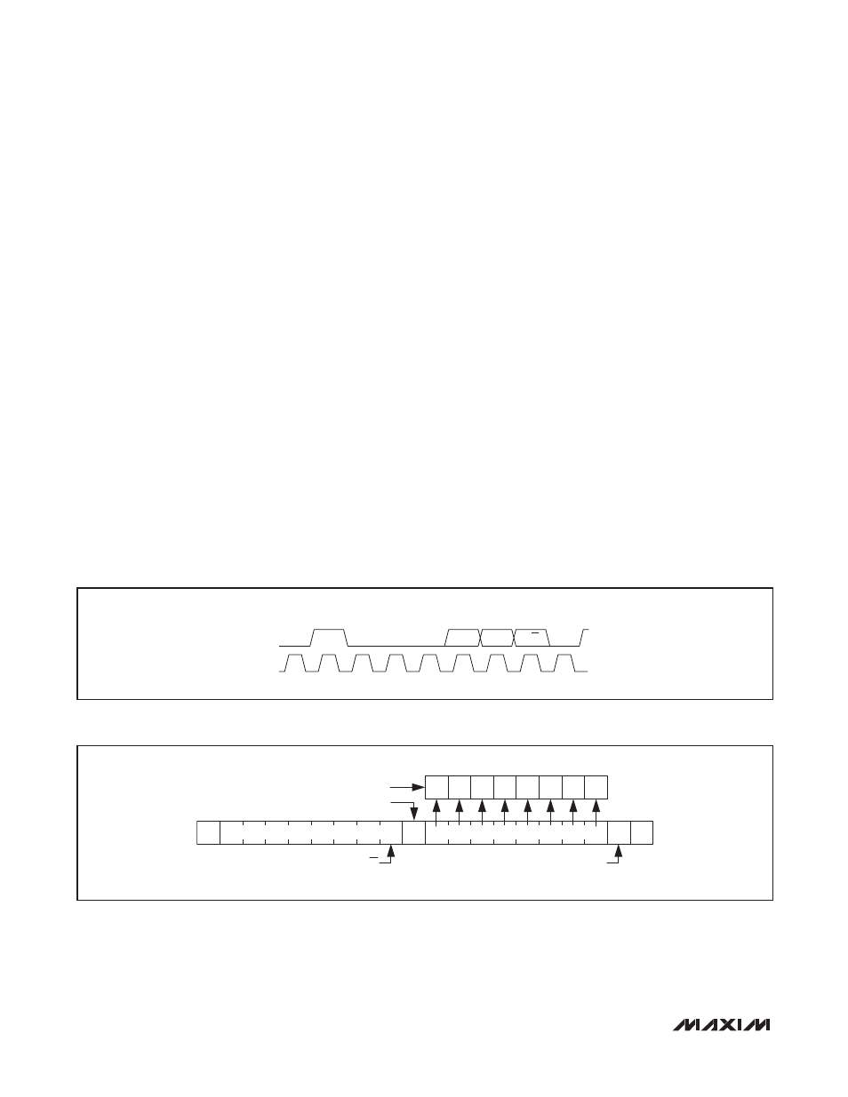
The MAX5971B has a 7-bit long slave address (Figure
10). The bit following the 7-bit slave address (bit 8) is the
R/W bit, which is low for a write command and high for a
read command. The upper five bits of the slave address
cannot be changed and are always [01000]. Using the
AD0 input, the lowest two bits can be programmed to
assign the MAX5971B one of 4 unique slave addresses
(see Table 5). The MAX5971B monitors the bus con-
tinuously, waiting for a START condition followed by the
MAX5971B’s slave address. When a MAX5971B rec-
ognizes its slave address, it acknowledges and is then
ready for continued communication.
Global Addressing and Alert Response Protocol
The global address call is used in writing mode to write
the same register to multiple devices (address 0x60).
In read mode (address 0x61), the global address call is
used as the alert response address. When responding
to a global call, the MAX5971B puts out on the data line
its own address whenever its interrupt is active (as does
every other device connected to the SDA line that has an
active interrupt). After every bit transmitted, the MAX5971B
checks that the data line effectively corresponds to the
data it is delivering. If it is not, it then backs off and frees
the data line. This litigation protocol always allows the
part with the lowest address to complete the transmis-
sion. The microcontroller then responds to that interrupt
and takes proper action. The MAX5971B does not reset
its own interrupt at the end of the alert response protocol.
The microcontroller has to do it by clearing the event
register through their CoR addresses or activating the
CLR_INT pushbutton (R1Ah[7]).
General Call
In compliance with the I
2
C specification, the MAX5971B
responds to the general call through the global address 30h.
Message Format for Writing the MAX5971B
A write to the MAX5971B comprises the device slave
address transmission with the R/W bit set to 0, followed by
at least one byte of information. The first byte of informa-
tion is the command byte (Figure 11). The command byte
determines which register of the MAX5971B is written to
by the next byte, if received. If the MAX5971B detects a
STOP condition after receiving the command byte but
before receiving any data, then the MAX5971B takes no
further action beyond storing the command byte.
Figure 10. Slave Address
Figure 11. Write Format: Control Byte Received
SDA
0
SCL
1
0
0
0
X
LSB
MSB
X
R/W
ACK
R/W
CB7
S
0
P
ACK
ACK
CB6 CB5 CB4 CB3 CB2 CB1 CB0
CONTROL BYTE STORED ON STOP CONDITION
ACKNOWLEDGE FROM THE MAX5971B
SLAVE ADDRESS
CONTROL BYTE
ACKNOWLEDGE FROM THE MAX5971B