Table 5. programmable device address settings – Rainbow Electronics MAX5971B User Manual
Page 22
22 _____________________________________________________________________________________
MAX5971B
Single-Port, 40W, IEEE 802.3af/at,
PSE Controller with I
2
C
The MAX5971B also contains an internal square wave,
PWM signal generator. The PWM runs at a typical fre-
quency of 25kHz with a default duty cycle of 6.25%.
The duty cycle is programmable from 6.25% up to 25%
through the PWM_TH[1:0] bits (R24h[5:4], Tables 33
and 34). PWMEN is used to enable or disable the PWM.
PWMEN is internally pulled up to the digital supply, and
can be left unconnected to enable the internal PWM.
When enabled, the LED pulses are driven by the PWM
to reduce the power dissipation and increase the system
efficiency. Force PWMEN low to disable the internal
PWM; LED is then driven directly.
Thermal Shutdown
If the MAX5971B die temperature reaches +150NC (typ),
an overtemperature fault is generated and the device
shuts down. The die temperature must cool down below
130NC (typ) to remove the overtemperature fault con-
dition. After a thermal shutdown condition clears, the
device is reset.
Watchdog
The R1Eh and R1Fh registers control the watchdog
operation. The watchdog function, when enabled, allows
the MAX5971B to automatically take over control and
securely shut down the power to the port in case of
software/firmware crashes. See the Register Map and
Description section for register configuration and set-
tings (Tables 29, 30, and 31).
Device Address (AD0)
The MAX5971B is programmable to one of four unique
slave addresses. To program the device address,
connect AD0 to V
EE
, SCL, SDA or to an external V
CC
supply referenced to V
EE
. This external V
CC
(at AD0)
must exceed the digital input logic-high threshold (V
CC
> 2.4V, see Table 5), but should not exceed 5.5V. An
external regulated 3.3V or 5V supply is recommended
for V
CC
.
I
2
C-Compatible Serial Interface
The MAX5971B operates as a slave that sends and
receives data through an I²C-compatible 2-wire inter-
face. The interface uses a serial-data line (SDA) and
a serial-clock line (SCL) to achieve communication
between master(s) and slave(s). A master (typically a
microcontroller) initiates all data transfers to and from the
MAX5971B, and generates the SCL clock that synchro-
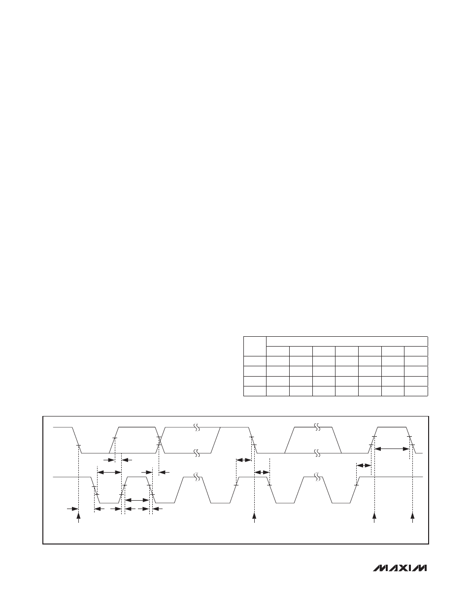
nizes the data transfer (see Figure 6).
The MAX5971B SDA line operates as both an input and
an output. A pullup resistor, typically 4.7kI, may be
required on SDA. The MAX5971B SCL line operates only
as an input. A pullup resistor may be required (typically
4.7kI) on SCL if there are multiple masters, or if the
master in a single-master system has an open-drain SCL
output.
Figure 6. 2-Wire Serial Interface Timing Details
Table 5. Programmable Device Address
Settings
SDA
SCL
t
SU,DAT
t
HD,DAT
t
LOW
t
SU,STA
t
HD,STA
t
R
t
F
START
CONDITION
REPEATED
START CONDITION
STOP
CONDITION
START
CONDITION
t
HD,STA
t
SU,STO
t
BUF
t
HIGH
AD0
DEVICE ADDRESS
A7
A6
A5
A4
A3
A2
A1
V
EE
0
1
0
0
0
0
0
V
CC
0
1
0
0
0
0
1
SCL
0
1
0
0
0
1
0
SDA
0
1
0
0
0
1
1