Pin description (continued) – Rainbow Electronics MAX5971B User Manual
Page 13
______________________________________________________________________________________ 13
MAX5971B
Single-Port, 40W, IEEE 802.3af/at,
PSE Controller with I
2
C
Pin Description (continued)
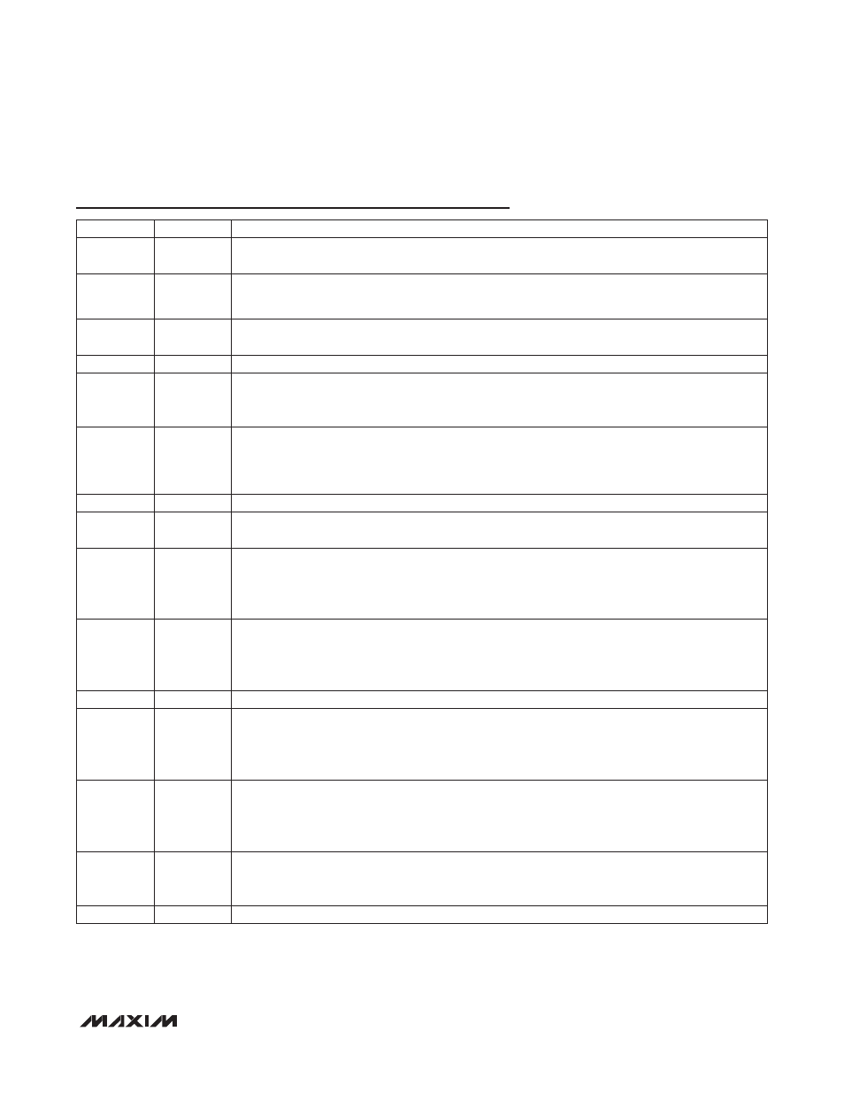
PIN
NAME
FUNCTION
9
SCL
2-Wire Serial Interface Input Clock Line. Referenced to V
EE
. Connect to V
EE
if the I
2
C interface is
not used.
10
INT
Open-Drain Interrupt Output. Referenced to V
EE
. INT is pulled low whenever an interrupt is sent to
the microcontroller. See the Interrupt section for details. Connect to V
EE
if the I
2
C interface is not
used.
11
AD0
Address Input. Referenced to V
EE
. AD0 is used to form the lower part of the device address. See
the Device Address section and Table 5 for details. Connect to V
EE
if the I
2
C interface is not used.
12
V
EE_DIG
Digital Low-Side Supply Input. Connect to V
EE
externally.
13
LEGACY
Legacy Detection Logic Input. Referenced to V
EE
. LEGACY is internally pulled up to the digital
supply. Leave unconnected to activate the legacy PD detection. Force low to disable this function.
The LEGACY logic level latches after the device is powered up or after a reset condition.
14
EN
Enable Input. Referenced to V
EE
. EN is internally pulled up to the digital supply. Leave uncon-
nected to enable the device. Force low for at least 40Fs to reset the device. The MIDSPAN, OSC,
and LEGACY states latch-in when the reset condition is removed (low-to-high transition). Bypass
EN to V
EE
with a 1nF ceramic capacitor.
15
I.C.
Internally Connected. Connect I.C. to V
EE
.
16, 18, 20,
22, 24, 28
N.C.
No Connection. Not internally connected. Leave N.C. unconnected.
17
LED
LED Indicator Open-Drain Output. Referenced to V
EE
. LED can sink 10mA and can drive an exter-
nal LED directly. Blinking functionality is provided to signal different conditions (see the PWM and
LED Signals section). Connect LED to AGND externally (see Figures 15 and 16) or to an external
supply (if available) through a series resistance.
19
OSC
AC-Disconnect Triangular Wave Output. Bypass with a 100nF (Q10% tolerance) external capacitor
to V
EE
to enable the AC disconnect function. Connect OSC to V
EE
to disable the AC disconnect
function and to activate the DC disconnect function. The OSC state latches after the device is
powered up or after a reset condition.
21
AGND
High-Side Supply Input
23
DET
Detection/Classification Voltage Output. DET is used to set the detection and classification probe
voltages and for the AC current sensing when using the AC disconnect function. To use the AC
disconnect function, place a 1kI and 0.47FF RC series in parallel with the external protection
diode to OUTP (see Figure 16).
25
OUTP
Port Pullup Output. OUTP is used to pull up the port voltage to AGND when needed. If AC dis-
connect is used, connect OUTP to the anode of the AC-blocking diode. If AC disconnect is not
used, connect OUTP to OUT (see Figures 15 and 17). Bypass OUTP to AGND with a 100V, 0.1FF
ceramic capacitor.
26, 27
OUT
Integrated MOSFET Output. If DC disconnect is used, connect the port output to OUTP (see
Figures 15 and 17). If the AC disconnect function is used, connect OUT to the cathode of the
AC-blocking diode (see Figure 16).
—
EP
Exposed Pad. Connect EP to V
EE
externally. See the Layout Procedure section for details.