Rainbow Electronics MAX5970 User Manual
Page 28

0V to 16V, Dual Hot-Swap Controller with 10-Bit
Current and Voltage Monitor and 4 LED Drivers
MAX5970
28 _____________________________________________________________________________________
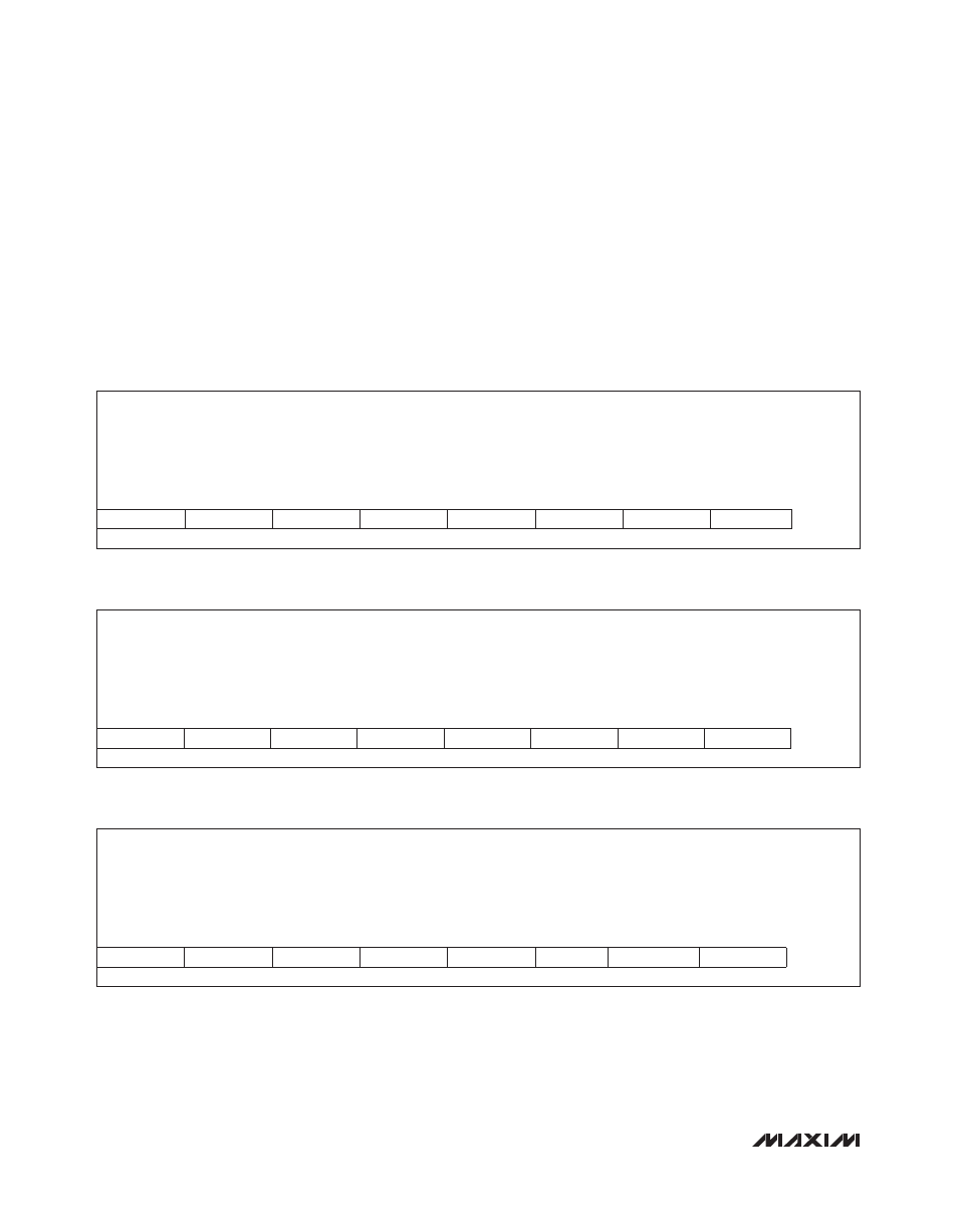
Table 32. ADC Minimum Voltage Conversion Register Format (High-Order Bits)
Table 33. ADC Minimum Voltage Conversion Register Format (Low-Order Bits)
Table 34. ADC Maximum Voltage Conversion Register Format (High-Order Bits)
Minimum and Maximum Value Detection
for Voltage Measurement Values
All voltage measurement values are compared with the
contents of minimum- and maximum-value registers,
and if the most recent measurement exceeds the stored
maximum or is less than the stored minimum, the corre-
sponding register is updated with the new value. These
peak detection registers are read accessible through the
I
2
C interface (see Tables 32–35). The minimum-value
registers are reset to 0x3FF, and the maximum-value
registers are reset to 0x000. These reset values are
loaded upon startup of a channel or at any time as com-
manded by register peak_log_rst (see Table 36).
Description:
Minimum voltage conversion result, high-order bits [9:2]
Register Title:
min_ch0_mon_msb
min_ch1_mon_msb
Register Addresses:
0x0C
0x14
R/W
R/W
R/W
R/W
R/W
R/W
R/W
R/W
RESET
VALUE
vmin_9
vmin_8
vmin_7
vmin_6
vmin_5
vmin_4
vmin_3
vmin_2
0xFF
bit 7
bit 6
bit 5
bit 4
bit 3
bit 2
bit 1
bit 0
Description:
Minimum voltage conversion result, low-order bits [1:0]
Register Title:
min_ch0_mon_lsb
min_ch1_mon_lsb
Register Addresses:
0x0D
0x15
R/W
R/W
R/W
R/W
R/W
R/W
R/W
R/W
RESET
VALUE
vmin_1
vmin_0
0x03
bit 7
bit 6
bit 5
bit 4
bit 3
bit 2
bit 1
bit 0
Description:
Maximum voltage conversion result, high-order bits [9:2]
Register Title:
max_ch0_mon_msb
max_ch1_mon_msb
Register Addresses:
0x0E
0x12
R
R
R
R
R
R
R/W
R/W
RESET
VALUE
vmax_9
vmax_8
vmax_7
vmax_6
vmax_5
vmax_4
vmax_3
vmax_2
0x00
bit 7
bit 6
bit 5
bit 4
bit 3
bit 2
bit 1
bit 0
