Electrical characteristics, Absolute maximum ratings – Rainbow Electronics MAX5970 User Manual
Page 2
0V to 16V, Dual Hot-Swap Controller with 10-Bit
Current and Voltage Monitor and 4 LED Drivers
MAX5970
2 ______________________________________________________________________________________
Stresses beyond those listed under “Absolute Maximum Ratings” may cause permanent damage to the device. These are stress ratings only, and functional
operation of the device at these or any other conditions beyond those indicated in the operational sections of the specifications is not implied. Exposure to absolute
maximum rating conditions for extended periods may affect device reliability.
IN, SENSE_, MON_, GATE_ to AGND ..................-0.3V to +30V
LED_ to AGND ......................................................-0.3V to +16V
ON_, SDA, SCL to AGND ........................................-0.3V to +6V
REG, DREG, IRNG_, MODE, PROT, A_,
PG_, ALERT, FAULT_ to AGND ................................ -0.3V to +4V
REG to DREG .......................................................-0.3V to +0.3V
RETRY, HWEN, POL to AGND ................-0.3V to (V
REG
+ 0.3V)
GATE1 to MON1, GATE2 to MON2 ........................-0.3V to +6V
GND_, DGND to AGND .......................................-0.3V to +0.3V
SDA, ALERT Current ....................................... -20mA to +50mA
LED_ Current ................................................. -20mA to +100mA
GATE_, MON_, GND_ Current .........................................750mA
All Other Pins Input/Output Current ...................................20mA
Continuous Power Dissipation (T
A
= +70NC)
36-Pin, 6mm x 6mm TQFN
(derate 35.7mW/°C above +70°C).......................... 2857mW**
Junction-to-Ambient Thermal Resistance (B
JA
) (Note 1) .. 28NC/W
Operating Temperature Range .......................... -40NC to +85NC
Junction Temperature .....................................................+150NC
Storage Temperature Range ............................ -65NC to +150NC
Lead Temperature (soldering, 10s) ................................+300NC
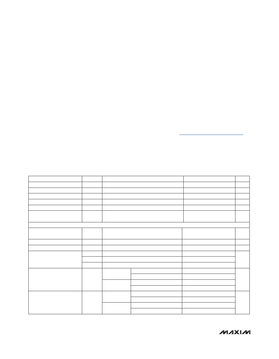
ELECTRICAL CHARACTERISTICS
(V
IN
= 2.7V to 16V, T
A
= -40NC to +85NC, unless otherwise noted. Typical values are at V
IN
= 3.3V and T
A
= +25NC.) (Note 2)
ABSOLUTE MAXIMUM RATINGS
Note 1: Package thermal resistances were obtained using the method described in JEDEC specification JESD51-7, using a four-
layer board. For detailed information on package thermal consideration, refer to
**As per JEDEC51 Standard (Multilayer Board)
PARAMETER
SYMBOL
CONDITIONS
MIN
TYP
MAX
UNITS
Supply Input-Voltage Range
V
IN
2.7
16
V
Hot-Swap Voltage Range
0
16
V
Supply Current
I
IN
2.5
4
mA
Internal LDO Output Voltage
REG
I
REG
= 0 to 5mA, V
IN
= 2.7V to 16V
2.49
2.53
2.6
V
Undervoltage Lockout
UVLO
V
IN
rising
2.7
V
Undervoltage Lockout
Hysteresis
UVLO
HYS
100
mV
CURRENT-MONITORING FUNCTION
MON_, SENSE_ Input-Voltage
Range
0
16
V
SENSE_ Input Current
V
SENSE_
, V
MON_
= 16V
32
75
F
A
MON_ Input Current
V
SENSE_
, V
MON_
= 16V
180
280
F
A
Current Measurement LSB
Voltage
25mV range
24.34
F
V
50mV range
48.39
100mV range
96.77
Current Measurement Error
(25mV Range)
V
MON_
= 0V
V
SENSE_
- V
MON_
= 5mV
-6.57
+6.22
% FS
V
SENSE_
- V
MON_
= 20mV
-6.71
+6.82
V
MON_
= 2.5V
to 16V
V
SENSE_
- V
MON_
= 5mV
-9.71
+8.92
V
SENSE_
- V
MON_
= 20mV
-10.24
+9.36
Current Measurement Error
(50mV Range)
V
MON_
= 0V
V
SENSE_
- V
MON_
= 10mV
-4.24
+3.78
% FS
V
SENSE_
- V
MON_
= 40mV
-4.53
+5.36
V
MON_
= 2.5V
to 16V
V
SENSE_
- V
MON_
= 10mV
-4.50
+4.00
V
SENSE_
- V
MON_
= 40mV
-4.20
+4.50