Rainbow Electronics MAX5970 User Manual
Page 13
0V to 16V, Dual Hot-Swap Controller with 10-Bit
Current and Voltage Monitor and 4 LED Drivers
MAX5970
______________________________________________________________________________________ 13
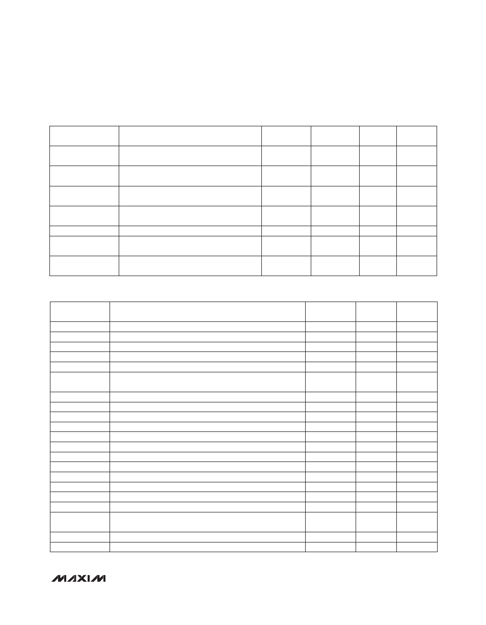
Table 1a. Register Address Map (Channel Specific) (continued)
Table 1b. Register Address Map (General)
REGISTER
DESCRIPTION
CHANNEL 1
CHANNEL 2
RESET
VALUE
READ/
WRITE
ov2thr_chx_msb
High 8 bits ([9:2]) of overvoltage critical
(OV2) threshold
0x20
0x2A
0xFF
R/W
ov2thr_chx_ lsb
Low 2 bits ([1:0]) of overvoltage critical
(OV2) threshold
0x21
0x2B
0x03
R/W
oithr_chx_msb
High 8 bits ([9:2]) of overcurrent warning
threshold
0x22
0x2C
0xFF
R/W
oithr_chx_ lsb
Low 2 bits ([1:0]) of overcurrent warning
threshold
0x23
0x2D
0x03
R/W
dac_chx-fast
Fast-comparator threshold DAC setting
0x2E
0x2F
0xBF
R/W
cubf_ba_chx_v
Base address for block read of 50-sample
voltage-signal data buffer
0x46
0x48
—
R
cubf_ba_chx_i
Base address for block read of 50-sample
current-signal data buffer
0x47
0x49
—
R
REGISTER
DESCRIPTION
ADDRESS
(HEX CODE)
RESET
VALUE
READ/
WRITE
mon_range
MON input range setting
0x18
0x00
R/W
cbuf_chx_store
Selective enabling of circular buffer
0x19
0x0F
R/W
ifast2slow
Current threshold fast-to-slow ratio setting
0x30
0x0F
R/W
status0
Slow-trip and fast-trip comparators status register
0x31
0x00
R
status1
PROT, MODE, and ON_ inputs status register
0x32
—
R
status2
Fast-trip threshold maximum range setting bits, from IRNG_
three-state inputs
0x33
—
R/W
status3
LATCH, POL, ALERT, and PG_ status register
0x34
—
R
fault0
Status register for undervoltage detection (warning or critical)
0x35
0x00
R/C
fault1
Status register for overvoltage detection (warning or critical)
0x36
0x00
R/C
fault2
Status register for overcurrent detection (warning)
0x37
0x00
R/C
pgdly
Delay setting between MON measurement and PG_ assertion
0x38
0x00
R/W
fokey
Load register with 0xA5 to enable force-on function
0x39
0x00
R/W
foset
Register that enables force-on function for a channel
0x3A
0x00
R/W
chxen
Channel enable bits
0x3B
—
R/W
dgl_i
OC deglitch enable bits
0x3C
0x00
R/W
dgl_uv
UV deglitch enable bits
0x3D
0x00
R/W
dgl_ov
OV deglitch enable bits
0x3E
0x00
R/W
cbufrd_hibyonly
Circular buffers readout mode: 8 bit or 10 bit
0x3F
0x0F
R/W
cbuf_dly_stop
Circular buffer stop-delay. Number of samples recorded to the
circular buffer after channel shutdown.
0x40
0x19
R/W
peak_log_rst
Reset control bits for peak-detection registers
0x41
0x00
R/W
peak_log_hold
Hold control bits for peak-detection registers
0x42
0x00
R/W