Rainbow Electronics MAX5970 User Manual
Page 21

0V to 16V, Dual Hot-Swap Controller with 10-Bit
Current and Voltage Monitor and 4 LED Drivers
MAX5970
______________________________________________________________________________________ 21
Once the PG_ output is asserted, the most recent cur-
rent samples are continuously compared to the pro-
grammable overcurrent warning register values. If the
measured current value exceeds the warning level, the
ALERT output is asserted. The MAX5970 response to
this digital comparator is not altered by the setting of the
PROT input (Tables 11 and 12).
Minimum and Maximum Value
Detection for Current Measurement Values
All current measurement values from the ADC are
continuously compared with the contents of minimum-
and maximum-value registers, and if the most recent
measurement exceeds the stored maximum or is less
than the stored minimum, the corresponding register
is updated with the new value. These peak detection
registers are read accessible through the I
2
C interface
(Tables 13–16). The minimum-value registers are reset
to 0x3FF, and the maximum-value registers are reset
to 0x000. These reset values are loaded upon startup
of a channel or at any time as commanded by register
peak_log_rst (Table 36).
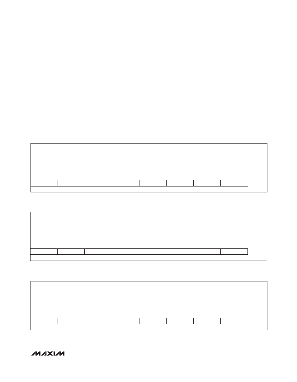
Table 11. Overcurrent Warning Threshold Register Format (High-Order Bits)
Table 13. ADC Minimum Current Conversion Register Format (High-Order Bits)
Table 12. Overcurrent Warning Threshold Register Format (Low-Order Bits)
Description:
Overcurrent warning threshold high-order bits [9:2]
Register Title:
oi_ch0_msb
oi_ch1_msb
Register Addresses:
0x22
0x2C
R/W
R/W
R/W
R/W
R/W
R/W
R/W
R/W
RESET
VALUE
oi_9
oi_8
oi_7
oi_6
oi_5
oi_4
oi_3
oi_2
0xFF
bit 7
bit 6
bit 5
bit 4
bit 3
bit 2
bit 1
bit 0
Description:
Overcurrent warning threshold low-order bits [1:0]
Register Title:
oi_ch0_ lsb
oi_ch1_lsb
Register Addresses:
0x23
0x2D
R
R
R
R
R
R
R/W
R/W
RESET
VALUE
oi_1
oi_0
0x03
bit 7
bit 6
bit 5
bit 4
bit 3
bit 2
bit 1
bit 0
Description:
Minimum current conversion result high-order bits [9:2]
Register Title:
min_ch0_cs_msb
min_ch1_cs_msb
Register Addresses:
0x08
0x10
R
R
R
R
R
R
R
R
RESET
VALUE
imin_9
imin_8
imin_7
imin_6
imin_5
imin_4
imin_3
imin_2
0xFF
bit 7
bit 6
bit 5
bit 4
bit 3
bit 2
bit 1
bit 0
