Rainbow Electronics MAX5970 User Manual
Page 16

0V to 16V, Dual Hot-Swap Controller with 10-Bit
Current and Voltage Monitor and 4 LED Drivers
MAX5970
16 _____________________________________________________________________________________
To determine the output dV/dt during startup, divide
the GATE_ pullup current I
G(UP)
by the gate-to-ground
capacitance. The voltage at the source of the external
MOSFET follows the gate voltage, so the load dV/dt is
the same as the gate dV/dt. Inrush current is the product
of the dV/dt and the load capacitance. The time to start
up t
SU
is the hot-swap voltage VS_ divided by the output
dV/dt.
Be sure to choose an external MOSFET that can handle
the power dissipated during startup. The inrush cur-
rent is roughly constant during startup, and the voltage
drop across the MOSFET (drain to source) decreases
linearly as the load capacitance charges. The resulting
power dissipation is therefore roughly equivalent to a
single pulse of magnitude (VS_ x Inrush current)/2 and
duration t
SU
. Refer to the thermal resistance charts in
the MOSFET data sheet to determine the junction tem-
perature rise during startup, and ensure that this does
not exceed the maximum junction temperature for worst-
case ambient conditions.
Circuit-Breaker Protection
As the channel is turned on and during normal opera-
tion, two analog comparators are used to detect an
overcurrent condition by sensing the voltage across
an external resistor connected between SENSE_ and
MON_. If the voltage across the sense resistor is less
than the slow-trip and fast-trip circuit-breaker thresholds,
the GATE_ output remains high. If either of the thresholds
is exceeded due to an overcurrent condition, the gate
of the MOSFET is pulled down to MON_ by an internal
500mA current source.
The higher of the two comparator thresholds, the fast-
trip, is set by an internal 8-bit DAC (see Table 8),
within one of three configurable full-scale current-sense
ranges: 25mV, 50mV, or 100mV (see Tables 7a and 7b).
The 8-bit fast-trip threshold DAC can be programmed
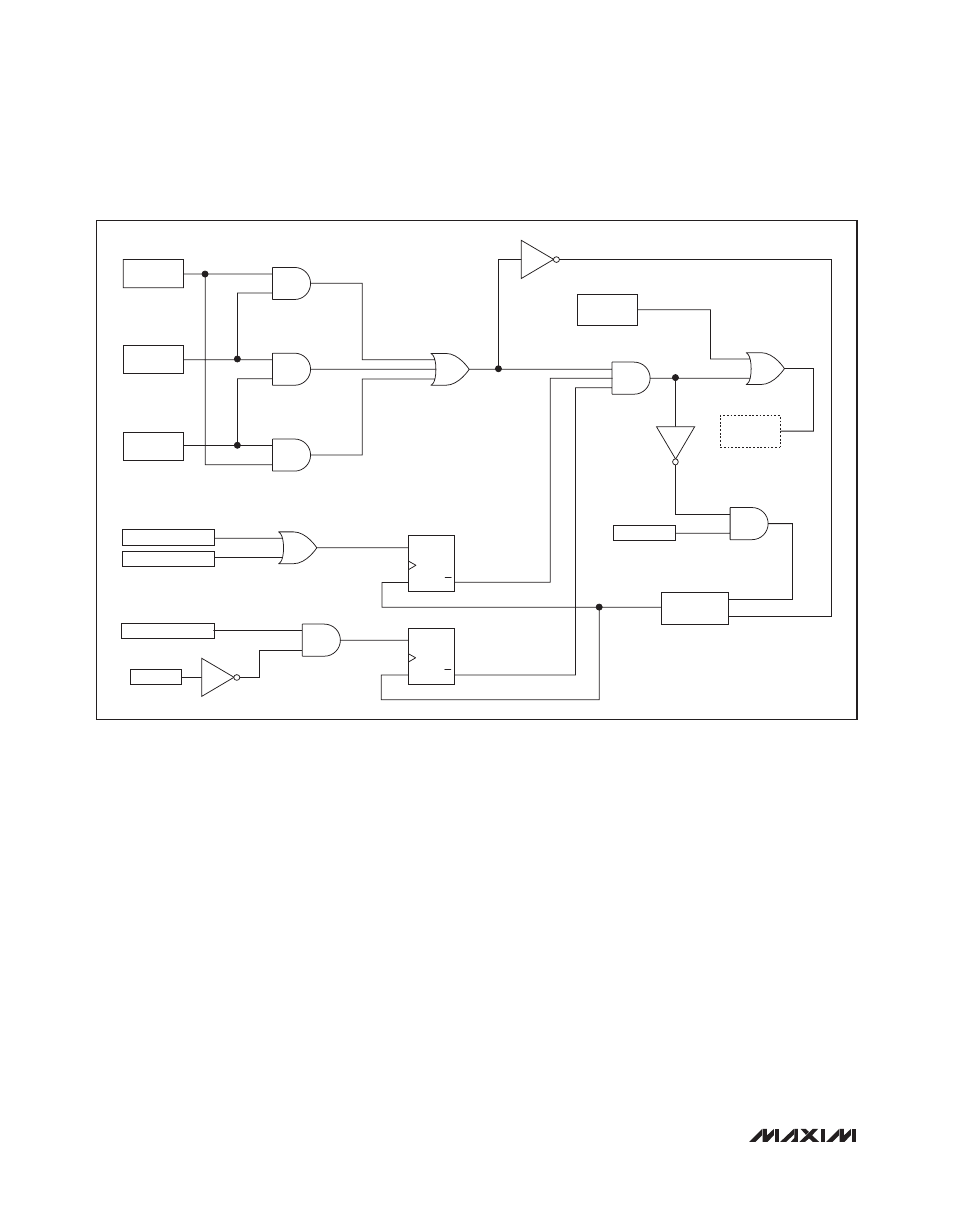
Figure 1. Channel On-Off Control Logic Functional Schematic
ON_
FORCE-ON
BIT
200ms DELAY,
THEN PULSE
CHANNEL
ENABLED
EN1_BIT
S
R
Q
Q
EN2_BIT
ANALOG SLOW_TRIP
RETRY PIN
ANALOG FAST_TRIP
UV/OV CRITICAL
PROT
S
R
Q
Q
