Rainbow Electronics MAX98089 User Manual
Simplified block diagram, General description, Features
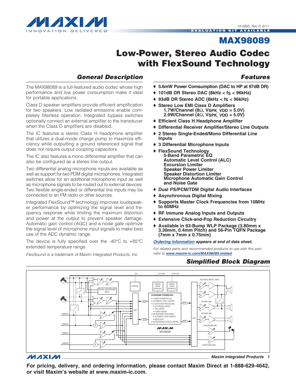
Table of contents
Document Outline
- General Description
- Features
- Simplified Block Diagram
- Functional Diagram
- Absolute Maximum Ratings
- Electrical Characteristics
- Digital Input/Output Characteristics
- Input Clock Characteristics
- Audio Interface Timing Characteristics
- Digital Microphone Timing Characterstics
- I2C Timing Characteristics
- Power Consumption
- Typical Operating Characteristics
- Pin Configuration
- Pin Description
- Detailed Description
- I2C Slave Address
- Registers
- Power Management
- Microphone Inputs
- Line Inputs
- ADC Input Mixers
- Record Path Signal Processing
- ADC Record Level Control
- Sidetone
- Digital Audio Interfaces
- Clock Control
- Sample Rate Converter
- Passband Filtering
- Playback Path Signal Processing
- Playback Level Control
- DAC Input Mixers
- Receiver Amplifier
- Speaker Amplifiers
- Speaker Amplifier Signal Processing
- Headphone
- Output Bypass Switches
- Click-and-Pop Reduction
- Jack Detection
- Battery Measurement
- Device Status
- I2C Serial Interface
- Device Revision
- Applications Information
- Ordering Information
- Package Information
- Revision History
- LIST OF FIGURES
- Figure 1. Non-TDM Audio Interface Timing
- Figure 2. TDM Audio Interface Timing Dia
- Figure 3. TDM Audio Interface Timing Dia
- Figure 4. Digital Microphone Timing Diag
- Figure 5. IC Interface Timing Diagram
- Figure 6. Microphone Input Block Diagram
- Figure 7. Line Input Block Diagram
- Figure 8. Summing Multiple Input Signals
- Figure 9. ADC Input Mixer Block Diagram
- Figure 10. Record Path Signal Processing
- Figure 12. AGC Timing
- Figure 13. ADC Record Level Control Bloc
- Figure 14. Sidetone Block Diagram
- Figure 15. Digital Audio Signal Routing
- Figure 16. Non-TDM Data Format Examples
- Figure 17. TDM Mode Data Format Examples
- Figure 18. Sample Rate Converter
- Figure 19. Digital Passband Filtering Bl
- Figure 21. ALC Input vs. Output Examples
- Figure 22. Maximum Recommended Filter Q
- Figure 23. Playback Level Control Block
- Figure 24. DAC Input Mixer Block Diagram
- Figure 25. Receiver Amplifier Block Diag
- Figure 26. Speaker Amplifier Path Block
- Figure 27. Speaker Amplifier Signal Proc
- Figure 28. Traditional Amplifier Output
- Figure 31. Headphone Amplifier Block Dia
- Figure 32. Output Bypass Switch Block Di
- Figure 33. Typical Configuration for Jac
- Figure 34. START, STOP, and REPEATED STA
- Figure 35. Acknowledge
- Figure 36. Writing One Byte of Data to t
- Figure 38. Reading One Byte of Data from
- Figure 39. Reading n Bytes of Data from
- Figure 41. Typical Application Circuit U
- Figure 42. Optional Class D Ferrite Bead
- Figure 43. Suggested Routing for the MAX
- Figure 44. MAX98089EWY WLP Ball Dimensio
- LIST OF TABLES
- Table 1. Register Map
- Table 2. Power Management Registers
- Table 3. Microphone Input Registers
- Table 4. Line Input Registers
- Table 5. ADC Input Mixer Register
- Table 6. Record Path Signal Processing R
- Table 7. ADC Record Level Control Regist
- Table 8. Sidetone Register
- Table 9. Common Digital Audio Formats
- Table 10. Digital Audio Interface Regist
- Table 11. Clock Control Registers
- Table 12. Common NI1/NI2 Values
- Table 13. Sample Rate Converter Register
- Table 14. Passband Filtering Registers
- Table 15. Voice Highpass Filters
- Table 16. Automatic Level Control Regist
- Table 17. EQ Registers
- Table 18. DAC Playback Level Control Reg
- Table 19. DAC Input Mixer Register
- Table 20. Receiver Output Mixer Register
- Table 21. Receiver Output Level Register
- Table 22. Speaker Output Mixer Register
- Table 23. Speaker Output Level Register
- Table 24. Excursion Limiter Registers
- Table 25. Power Limiter Registers
- Table 26. Distortion Limiter Registers
- Table 27. Headphone Output Mixer Registe
- Table 28. Headphone Output Level Registe
- Table 29. Output Bypass Switches Registe
- Table 30. Click-and-Pop Reduction Regist
- Table 31. Change in JKSNS Upon Jack Inse
- Table 32. Change in JKSNS Upon Button Pr
- Table 33. Change in JKSNS Upon Jack Remo
- Table 34. Jack Detection Registers
- Table 34. Jack Detection Registers (cont
- Table 35. Battery Measurement Registers
- Table 36. Status and Interrupt Registers
- Table 37. Device Revision Register
- Table 38. Example Startup Sequence
- Table 39. Registers That Are Sensitive t
- Table 40. Unused Pins