Rainbow Electronics MAX98089 User Manual
Simplified block diagram, General description, Features
MAX98089
Low-Power, Stereo Audio Codec
with FlexSound Technology
����������������������������������������������������������������� Maxim Integrated Products 1
19-5865; Rev 0; 6/11
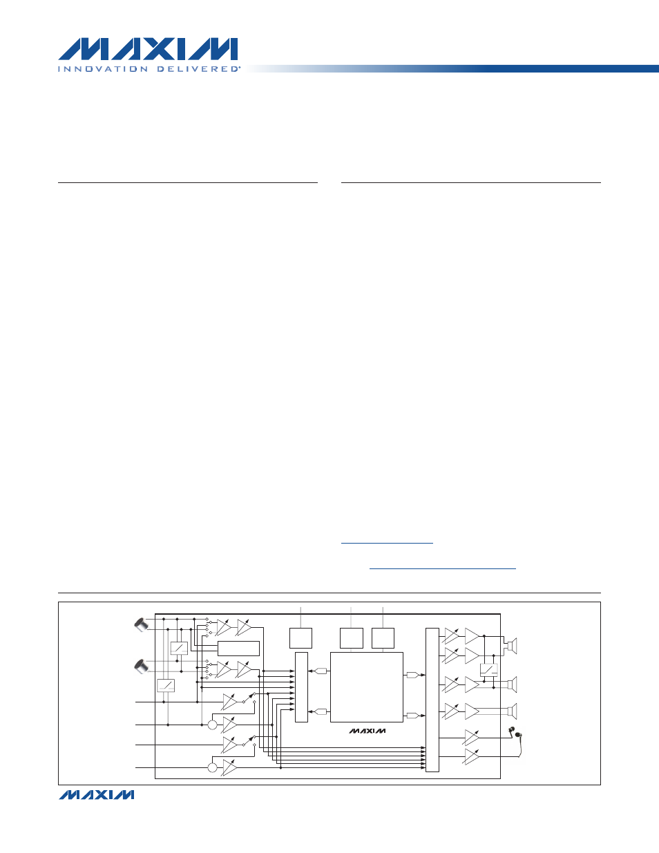
Simplified Block Diagram
For related parts and recommended products to use with this part,
refer to
www.maxim-ic.com/MAX98089.related
.
FlexSound is a trademark of Maxim Integrated Products, Inc.
General Description
The MAX98089 is a full-featured audio codec whose high
performance and low power consumption make it ideal
for portable applications.
Class D speaker amplifiers provide efficient amplification
for two speakers. Low radiated emissions enable com-
pletely filterless operation. Integrated bypass switches
optionally connect an external amplifier to the transducer
when the Class D amplifiers are disabled.
The IC features a stereo Class H headphone amplifier
that utilizes a dual-mode charge pump to maximize effi-
ciency while outputting a ground referenced signal that
does not require output coupling capacitors.
The IC also features a mono differential amplifier that can
also be configured as a stereo line output.
Two differential analog microphone inputs are available as
well as support for two PDM digital microphones. Integrated
switches allow for an additional microphone input as well
as microphone signals to be routed out to external devices.
Two flexible single-ended or differential line inputs may be
connected to an FM radio or other sources.
Integrated FlexSoundK technology improves loudspeak-
er performance by optimizing the signal level and fre-
quency response while limiting the maximum distortion
and power at the output to prevent speaker damage.
Automatic gain control (AGC) and a noise gate optimize
the signal level of microphone input signals to make best
use of the ADC dynamic range.
The device is fully specified over the -40NC to +85NC
extended temperature range.
Features
S
5.6mW Power Comsumption (DAC to HP at 97dB DR)
S
101dB DR Stereo DAC (8kHz < f
S
< 96kHz)
S
93dB DR Stereo ADC (8kHz < f
S
< 96kHz)
S
Stereo Low EMI Class D Amplifiers
1.7W/Channel (8I, V
SPK�VDD
= 5.0V)
2.9W/Channel (4I, V
SPK�VDD
= 5.0V)
S
Efficient Class H Headphone Amplifier
S
Differential Receiver Amplifier/Stereo Line Outputs
S
2 Stereo Single-Ended/Mono Differential Line
Inputs
S
3 Differential Microphone Inputs
S
FlexSound Technology
5-Band Parametric EQ
Automatic Level Control (ALC)
Excursion Limiter
Speaker Power Limiter
Speaker Distortion Limiter
Microphone Automatic Gain Control
and Noise Gate
S
Dual I
2
S/PCM/TDM Digital Audio Interfaces
S
Asynchronous Digital Mixing
S
Supports Master Clock Frequencies from 10MHz
to 60MHz
S
RF Immune Analog Inputs and Outputs
S
Extensive Click-and-Pop Reduction Circuitry
S
Available in 63-Bump WLP Package (3.80mm x
3.30mm, 0.4mm Pitch) and 56-Pin TQFN Package
(7mm x 7mm x 0.75mm)
E V A L U A T I O N K I T A V A I L A B L E
DIGITAL MICROPHONE
INPUT
+
+
LINEIN A1
LINEIN A2
LINEIN B1
LINEIN B2
DAC
DAC
MIX
RECEIVER/LINEOUT AMPS
SPEAKER AMP
SPEAKER AMP
HEADPHONE AMP
HEADPHONE AMP
ADC
ADC
MIX
FLEXSOUND
TECHNOLOGY
• 5-BAND PARAMETRIC EQ
• AUTOMATIC LEVEL CONTROL
• LOUDSPEAKER PROCESSING
• EXCURSION LIMITER
• THD LIMITER
• POWER LIMITER
• MICROPHONE PROCESSING
• AUTOMATIC GAIN CONTROL
• NOISE GATE
• ASYNCHRONOUS DIGITAL MIXING
I
2
C
CONTROL
I
2
S/PCM
DIGITAL
AUDIO
INTERFACE
I
2
S/PCM
MAX98089
DIGITAL
AUDIO
INTERFACE
For pricing, delivery, and ordering information, please contact Maxim Direct at 1-888-629-4642,
or visit Maxim’s website at www.maxim-ic.com.
Document Outline
- General Description
- Features
- Simplified Block Diagram
- Functional Diagram
- Absolute Maximum Ratings
- Electrical Characteristics
- Digital Input/Output Characteristics
- Input Clock Characteristics
- Audio Interface Timing Characteristics
- Digital Microphone Timing Characterstics
- I2C Timing Characteristics
- Power Consumption
- Typical Operating Characteristics
- Pin Configuration
- Pin Description
- Detailed Description
- I2C Slave Address
- Registers
- Power Management
- Microphone Inputs
- Line Inputs
- ADC Input Mixers
- Record Path Signal Processing
- ADC Record Level Control
- Sidetone
- Digital Audio Interfaces
- Clock Control
- Sample Rate Converter
- Passband Filtering
- Playback Path Signal Processing
- Playback Level Control
- DAC Input Mixers
- Receiver Amplifier
- Speaker Amplifiers
- Speaker Amplifier Signal Processing
- Headphone
- Output Bypass Switches
- Click-and-Pop Reduction
- Jack Detection
- Battery Measurement
- Device Status
- I2C Serial Interface
- Device Revision
- Applications Information
- Ordering Information
- Package Information
- Revision History
- LIST OF FIGURES
- Figure 1. Non-TDM Audio Interface Timing
- Figure 2. TDM Audio Interface Timing Dia
- Figure 3. TDM Audio Interface Timing Dia
- Figure 4. Digital Microphone Timing Diag
- Figure 5. IC Interface Timing Diagram
- Figure 6. Microphone Input Block Diagram
- Figure 7. Line Input Block Diagram
- Figure 8. Summing Multiple Input Signals
- Figure 9. ADC Input Mixer Block Diagram
- Figure 10. Record Path Signal Processing
- Figure 12. AGC Timing
- Figure 13. ADC Record Level Control Bloc
- Figure 14. Sidetone Block Diagram
- Figure 15. Digital Audio Signal Routing
- Figure 16. Non-TDM Data Format Examples
- Figure 17. TDM Mode Data Format Examples
- Figure 18. Sample Rate Converter
- Figure 19. Digital Passband Filtering Bl
- Figure 21. ALC Input vs. Output Examples
- Figure 22. Maximum Recommended Filter Q
- Figure 23. Playback Level Control Block
- Figure 24. DAC Input Mixer Block Diagram
- Figure 25. Receiver Amplifier Block Diag
- Figure 26. Speaker Amplifier Path Block
- Figure 27. Speaker Amplifier Signal Proc
- Figure 28. Traditional Amplifier Output
- Figure 31. Headphone Amplifier Block Dia
- Figure 32. Output Bypass Switch Block Di
- Figure 33. Typical Configuration for Jac
- Figure 34. START, STOP, and REPEATED STA
- Figure 35. Acknowledge
- Figure 36. Writing One Byte of Data to t
- Figure 38. Reading One Byte of Data from
- Figure 39. Reading n Bytes of Data from
- Figure 41. Typical Application Circuit U
- Figure 42. Optional Class D Ferrite Bead
- Figure 43. Suggested Routing for the MAX
- Figure 44. MAX98089EWY WLP Ball Dimensio
- LIST OF TABLES
- Table 1. Register Map
- Table 2. Power Management Registers
- Table 3. Microphone Input Registers
- Table 4. Line Input Registers
- Table 5. ADC Input Mixer Register
- Table 6. Record Path Signal Processing R
- Table 7. ADC Record Level Control Regist
- Table 8. Sidetone Register
- Table 9. Common Digital Audio Formats
- Table 10. Digital Audio Interface Regist
- Table 11. Clock Control Registers
- Table 12. Common NI1/NI2 Values
- Table 13. Sample Rate Converter Register
- Table 14. Passband Filtering Registers
- Table 15. Voice Highpass Filters
- Table 16. Automatic Level Control Regist
- Table 17. EQ Registers
- Table 18. DAC Playback Level Control Reg
- Table 19. DAC Input Mixer Register
- Table 20. Receiver Output Mixer Register
- Table 21. Receiver Output Level Register
- Table 22. Speaker Output Mixer Register
- Table 23. Speaker Output Level Register
- Table 24. Excursion Limiter Registers
- Table 25. Power Limiter Registers
- Table 26. Distortion Limiter Registers
- Table 27. Headphone Output Mixer Registe
- Table 28. Headphone Output Level Registe
- Table 29. Output Bypass Switches Registe
- Table 30. Click-and-Pop Reduction Regist
- Table 31. Change in JKSNS Upon Jack Inse
- Table 32. Change in JKSNS Upon Button Pr
- Table 33. Change in JKSNS Upon Jack Remo
- Table 34. Jack Detection Registers
- Table 34. Jack Detection Registers (cont
- Table 35. Battery Measurement Registers
- Table 36. Status and Interrupt Registers
- Table 37. Device Revision Register
- Table 38. Example Startup Sequence
- Table 39. Registers That Are Sensitive t
- Table 40. Unused Pins