Applications information, Table 2. component values – Rainbow Electronics MAX19985A User Manual
Page 20

MAX19985A
Dual, SiGe, High-Linearity, 700MHz to 1000MHz
Downconversion Mixer with LO Buffer/Switch
20
______________________________________________________________________________________
Applications Information
Input and Output Matching
The RF and LO inputs are internally matched to 50
Ω. No
matching components are required. The RF port input
return loss is typically 20dB over the RF frequency range
of 770MHz to 915MHz and return loss at the LO ports are
typically 20dB over the entire LO range. RF and LO inputs
require only DC-blocking capacitors for interfacing.
The IF output impedance is 200
Ω (differential). For
evaluation, an external low-loss 4:1 (impedance ratio)
balun transforms this impedance to a 50
Ω single-ended
output (see the
Typical Application Circuit
).
Externally Adjustable Bias
Each channel of the MAX19985A has two pins (LO_BIAS,
IF_BIAS) that allow external resistors to set the internal
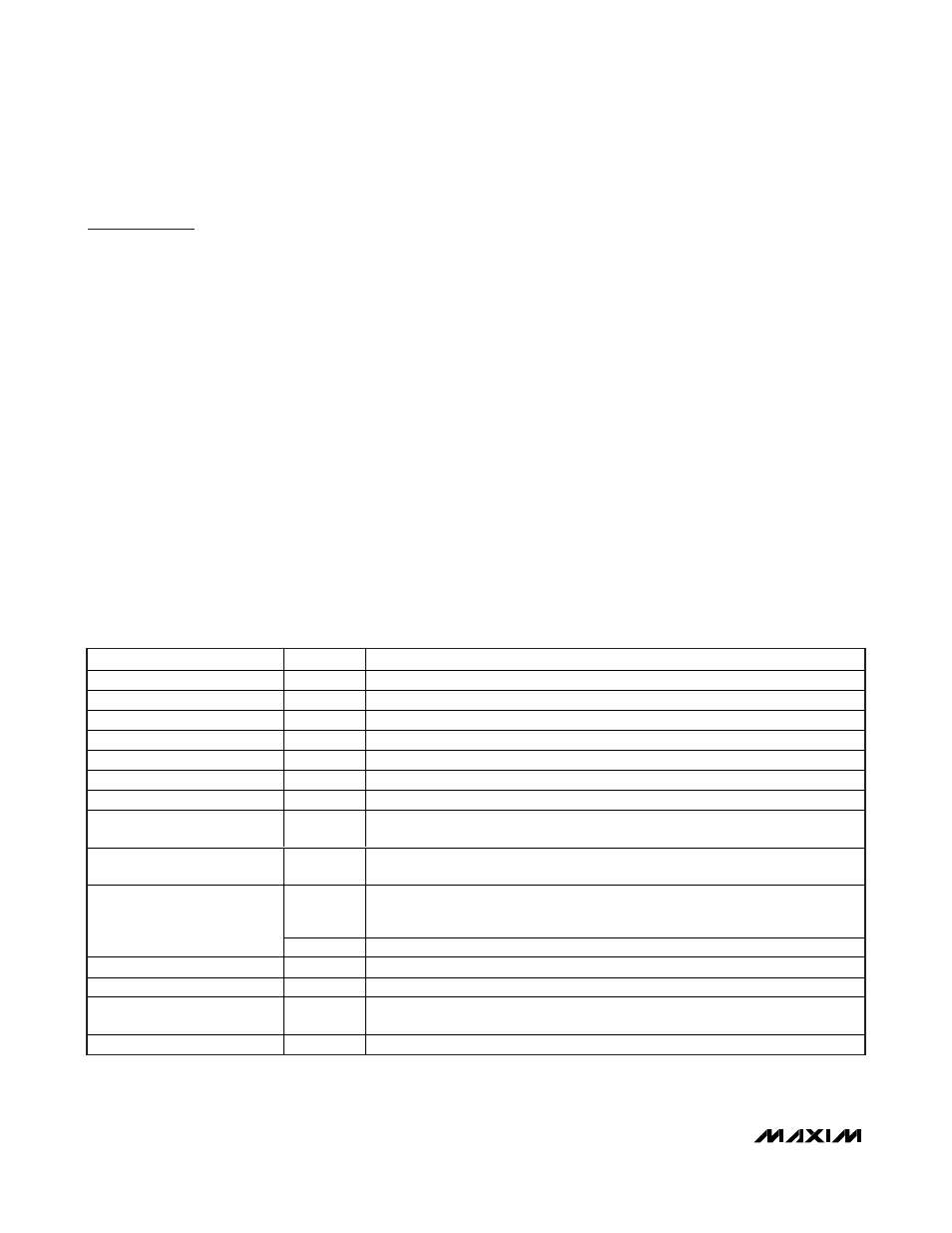
bias currents. Nominal values for these resistors are given
in Table 2. Larger-value resistors can be used to reduce
power dissipation at the expense of some performance
loss. See the
Typical Operating Characteristics
to evaluate
the power vs. performance tradeoff. If ±1% resistors are
not readily available, ±5% resistors can be substituted.
LEXT_ Inductors
For applications requiring optimum RF-to-IF and LO-to-
IF isolation, connect a parallel combination of a low-
ESR inductor and a 500
Ω resistor from LEXT_ (pins 15
and 31) to ground. When improved isolation is not
required, connect LEXT_ to ground using a 0
Ω resis-
tance. See the
Typical Operating Characteristics
to
evaluate the isolation vs. inductor value tradeoff.
Layout Considerations
A properly designed PCB is an essential part of any
RF/microwave circuit. Keep RF signal lines as short as
possible to reduce losses, radiation, and inductance.
The load impedance presented to the mixer must be so
that any capacitance from both IF- and IF+ to ground
does not exceed several picofarads. For the best perfor-
mance, route the ground pin traces directly to the
exposed pad under the package. The PCB exposed
pad MUST be connected to the ground plane of the
PCB. It is suggested that multiple vias be used to con-
nect this pad to the lower-level ground planes. This
method provides a good RF/thermal-conduction path for
the device. Solder the exposed pad on the bottom of the
Table 2. Component Values
COMPONENT
VALUE
DESCRIPTION
C1, C2, C7, C8
39pF
Microwave capacitors (0402)
C3, C6
0.033µF
Microwave capacitors (0603)
C4, C5
—
Not used
C9, C13, C15, C17, C18
0.01µF
Microwave capacitors (0402)
C10, C11, C12, C19, C20, C21
150pF
Microwave capacitors (0603)
C14, C16
82pF
Microwave capacitors (0402)
L1, L2, L4, L5
330nH
Wire-wound high-Q inductors (0805)
L3, L6
30nH
Wire-wound high-Q inductors (0603). Smaller values can be used at the expense of
some performance loss (see the Typical Operating Characteristics).
R1, R4
698
Ω
±1% resistors (0402). Larger values can be used to reduce power at the expense of
some performance loss (see the Typical Operating Characteristics).
1.2k
Ω
±1% resistors (0402). Use for V
CC
= +5.0V applications. Larger values can be used
to reduce power at the expense of some performance loss (see the Typical
Operating Characteristics).
R2, R5
600
Ω
±1% resistors (0402). Use for V
CC
= +3.3V applications.
R3, R6
0
Ω
±1% resistors (1206)
R7, R8
500
Ω
±1% resistors (0402)
T1, T2
4:1
Transformers (200:50)
Mini-Circuits TC4-1W-7A
U1
—
MAX19985A IC
