Rainbow Electronics MAX19995 User Manual
Page 7
MAX19995
Dual, SiGe, High-Linearity, 1700MHz to 2200MHz
Downconversion Mixer with LO Buffer/Switch
_______________________________________________________________________________________
7
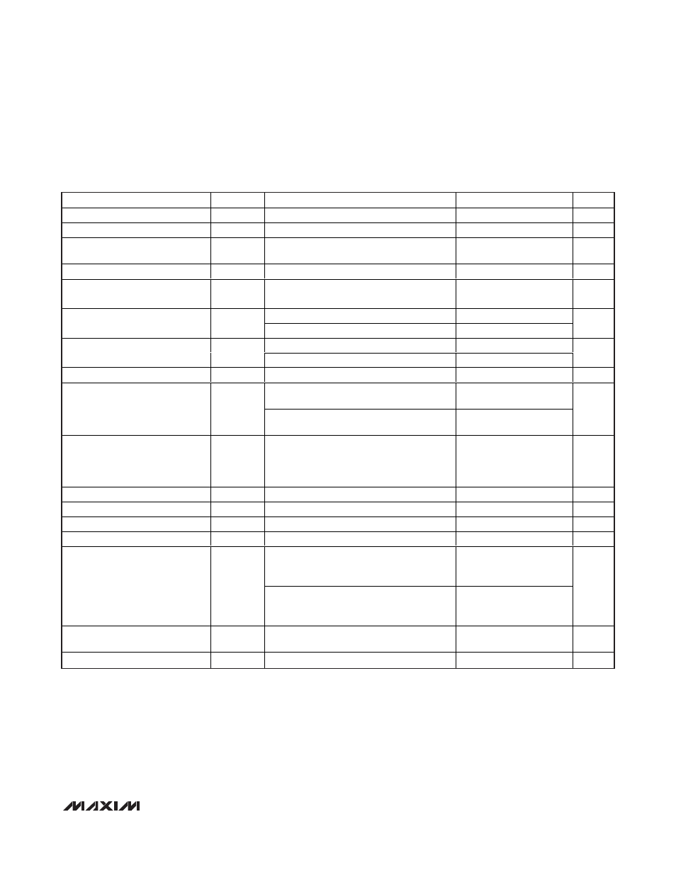
+3.3V SUPPLY AC ELECTRICAL CHARACTERISTICS (continued)
(
Typical Application Circuit. Typical values are at V
CC
= +3.3V, P
RF
= -5dBm, P
LO
= 0dBm, f
RF
= 1800MHz, f
LO
= 1610MHz,
f
IF
= 190MHz, T
C
= +25°C, unless otherwise noted.) (Note 6)
Note 5:
Not production tested. Operation outside this range is possible, but with degraded performance of some parameters. See
the
Typical Operating Characteristics.
Note 6:
All limits reflect losses of external components, including a 0.65dB loss at f
IF
= 190MHz due to the 4:1 impedance trans-
former. Output measurements were taken at IF outputs of the
Typical Application Circuit.
Note 7:
Maximum reliable continuous input power applied to the RF or IF port of this device is +12dBm from a 50
Ω source.
Note 8:
Guaranteed by design and characterization.
Note 9:
Measured with external LO source noise filtered so the noise floor is -174dBm/Hz. This specification reflects the effects of
all SNR degradations in the mixer, including the LO noise as defined in Application Note 2021:
Specifications and
Measurement of Local Oscillator Noise in Integrated Circuit Base Station Mixers.
Note 10: Limited production testing.
PARAMETER
SYMBOL
CONDITIONS
MIN
TYP
MAX
UNITS
Input Compression Point
IP
1dB
(Note 7)
8.9
dBm
Input Intercept Point
IIP3
f
RF1
- f
RF2
= 1MHz
18.5
dBm
Input Intercept Variation Over
Temperature
TC
IIP3
f
RF1
- f
RF2
= 1MHz, T
C
= -40°C to +85°C
0.0034
dBm/°C
Noise Figure
NF
SSB
Single sideband, no blockers present
9.0
dB
Noise Figure Temperature
Coefficient
TC
NF
Single sideband, no blockers present,
T
C
= -40°C to +85°C
0.016
dB/°C
P
RF
= -10dBm
73
2RF-2LO Spur Rejection
2 x 2
P
RF
= -5dBm
68
dBc
P
RF
= -10dBm
70
3RF-3LO Spur Rejection
3 x 3
P
RF
= -5dBm
60
dBc
RF Input Return Loss
LO on and IF terminated
21
dB
LO port selected, RF and IF terminated into
matched impedance
16
LO Input Return Loss
LO port unselected, RF and IF terminated
into matched impedance
20
dB
IF Return Loss
RF terminated into 50
Ω, LO driven by 50Ω
source, IF transformed to 50
Ω using
external components shown in Typical
Application Circuit, f
IF
= 190MHz
12.5
dB
RF-to-IF Isolation
42
dB
LO Leakage at RF Port
-40
dBm
2LO Leakage at RF Port
-29
dBm
LO Leakage at IF Port
-43
dBm
RFMAIN converted power measured at
IFD_, relative to IFM_, all unused ports
terminated to 50
Ω
49
Channel Isolation
RFDIV converted power measured at IFM_,
relative to IFD_, all unused ports terminated
to 50
Ω
49
dB
LO-to-LO Isolation
P
LO1
= +3dBm, P
LO2
= +3dBm,
f
LO1
= 1610MHz, f
LO2
= 1611MHz
55
dB
LO Switching Time
50% of LO S E L to IF settl ed w i thi n 2 d eg r ees
50
ns