Clock generation, Kb nv memory, Oscillator (differential) – Xilinx SP601 Hardware UG518 User Manual
Page 27
SP601 Hardware User Guide
27
UG518 (v1.1) August 19, 2009
Detailed Description
8-Kb NV Memory
The SP601 hosts a 8-Kb ST Microelectronics M24C08-WDW6TP IIC parameter storage
memory device (U7). The IIC address of U7 is 0b1010100, and U7 is not write protected
(WP pin 7 is tied to GND).
References
See the ST Micro M24C08-WDW6TP data sheet for more information at
.
In addition, see the Xilinx XPS IIC Bus Interface specification at
.
Also, see
“9. VITA 57.1 FMC-LPC Connector,” page 28
.
8. Clock Generation
There are three clock sources available on the
SP601
.
Oscillator (Differential)
The SP601 has one 2.5V LVDS differential 200 MHz oscillator (U5) soldered onto the board
and wired to an FPGA global clock input.
•
Crystal oscillator: Epson EG2121CA
•
PPM frequency jitter: 50 ppm
References
For more details, see the Epson data sheet at
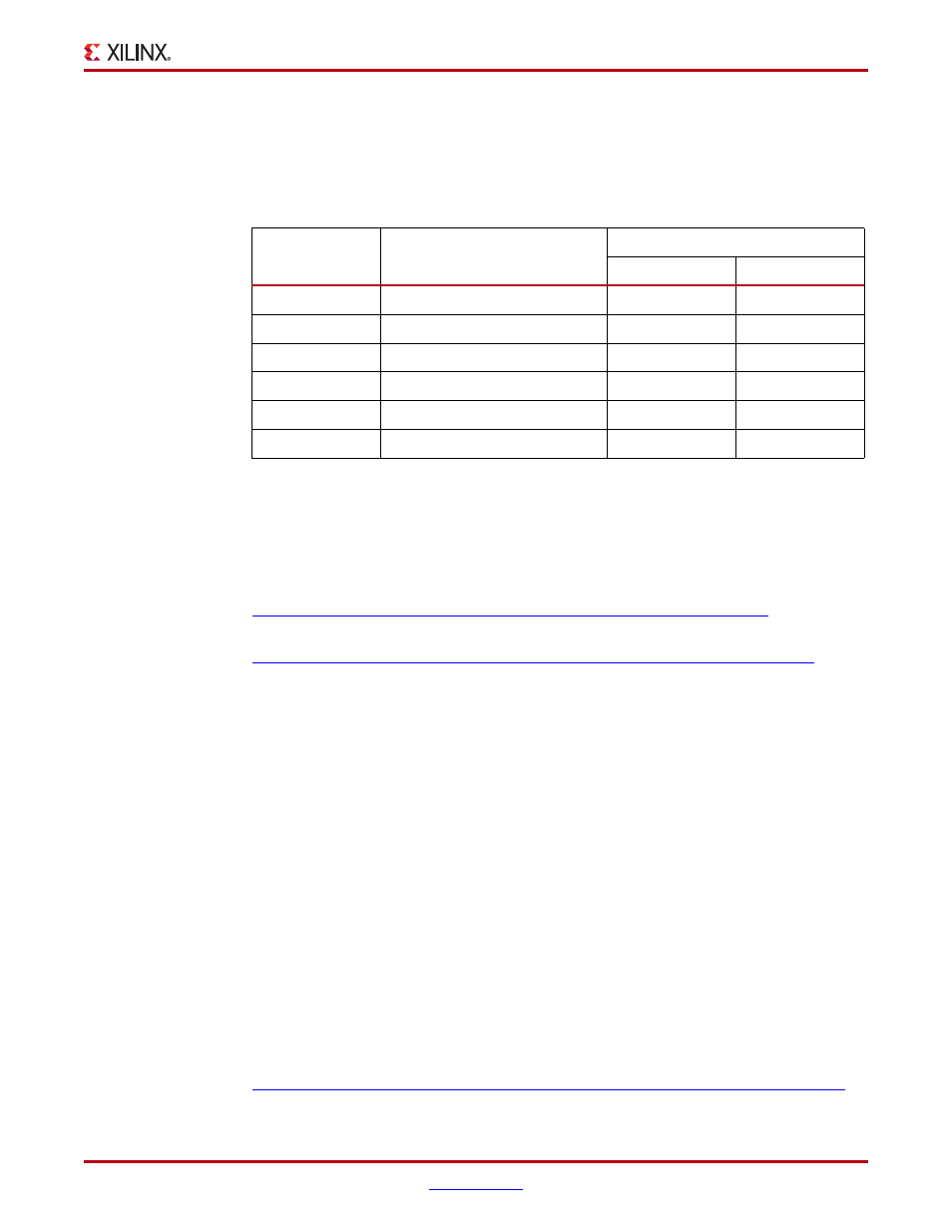
Table 1-12:
IIC Memory Connections
FPGA U1 Pin
Number
Schematic Netname
SPI Memory U7
Pin Number
Pin
Not Applicable
Tied to GND
1
A0
Not Applicable
Tied to GND
2
A1
Not Applicable
Pulled up (0 ohm) to VCC3V3
3
A2
N10
IIC_SDA_MAIN
5
SDA
P11
IIC_SCL_MAIN
6
SCL
Not Applicable
Tied to GND
7
WP
X-Ref Target - Figure 1-14
NET "IIC_SCL_MAIN"
LOC = "P11";
NET "IIC_SDA_MAIN"
LOC = "N10";
Figure 1-14:
UCF Location Constraints for IIC Connections
X-Ref Target - Figure 1-15
NET "SYSCLK_N" LOC = "K16";
NET "SYSCLK_P" LOC = "K15";
Figure 1-15:
UCF Location Constraints for Oscillator Connections