128 mb ddr2 component memory, Table 1-4 – Xilinx SP601 Hardware UG518 User Manual
Page 14
14
SP601 Hardware User Guide
UG518 (v1.1) August 19, 2009
Chapter 1: SP601 Evaluation Board
References
See the Xilinx Spartan-6 FPGA documentation for more information at
.
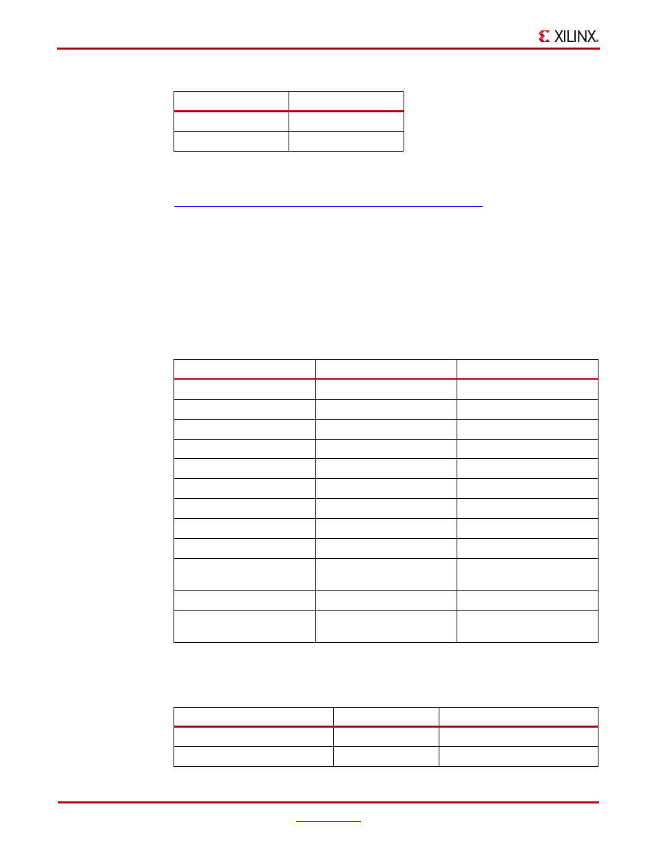
2. 128 MB DDR2 Component Memory
There are 128 MB of DDR2 memory available on the
SP601
board. A 1-Gb Elpida
EDE1116ACBG (84-ball) DDR2 memory component is accessible through Bank 3 of the
LX16 device. The Spartan-6 FPGA hard memory controller is used for data transfer across
the DDR2 memory interface's 16-bit data path using SSTL18 signaling. The maximum data
rate supported is 800 Mb/s with a memory clock running at 400 MHz. Signal integrity is
maintained through DDR2 resistor terminations and memory on-die terminations (ODT),
as shown in
Table 1-3
and
Table 1-4
.
2
2.5V
3
1.8V
Table 1-2:
I/O Voltage Rail of FPGA Banks (Cont’d)
FPGA Bank
I/O Voltage Rail
Table 1-3:
Termination Resistor Requirements
Signal Name
Board Termination
On-Die Termination
DDR2_A[14:0]
49.9 ohms to V
TT
DDR2_BA[2:0]
49.9 ohms to V
TT
DDR2_RAS_N
49.9 ohms to V
TT
DDR2_CAS_N
49.9 ohms to V
TT
DDR2_WE_N
49.9 ohms to V
TT
DDR2_CS_N
100 ohms to GND
DDR2_CKE
4.7K ohms to GND
DDR2_ODT
4.7K ohms to GND
DDR2_DQ[15:0]
ODT
DDR2_UDQS[P,N],
DDR2_LDQS[P,N]
ODT
DDR2_UDM, DDR2_LDM
ODT
DDR2_CK[P,N]
100 ohm differential at
memory component
Notes:
1. Nominal value of V
TT
for DDR2 interface is 0.9V.
Table 1-4:
FPGA On-Chip (OCT) Termination External Resistor Requirements
FPGA U1 Pin
FPGA Pin Number
Board Connection for OCT
ZIO
L6
No Connect
RZQ
C2
100 ohms to GROUND