Linear flash bpi – Xilinx SP601 Hardware UG518 User Manual
Page 20
20
SP601 Hardware User Guide
UG518 (v1.1) August 19, 2009
Chapter 1: SP601 Evaluation Board
Figure 1-8
provides the UCF constraints for the SPI serial flash PROM.
References
See the Winbond Serial Flash specifications for more information at
See the XPS Serial Peripheral Interface specification for more information at
4. Linear Flash BPI
An 8-bit (16 MB) Numonyx linear flash memory (TE 28F128J3D-75) (J3D type) is used to
provide non-volatile bitstream, code, and data storage. The J3D devices operate at 3.0V; the
Spartan-6 FPGA I/Os are 3.3V tolerant and provide electrically compatible logic levels to
directly access the linear flash BPI through a 2.5V bank. For details on configuring the
FPGA, see
X-Ref Target - Figure 1-8
NET "FPGA_D2_MISO3" LOC = "V14";
NET "SPI_CS_B" LOC = "V3";
NET "FPGA_D0_DIN_MISO_MISO1" LOC = "R13";
NET "FPGA_D1_MISO2" LOC = "T14";
NET "FPGA_MOSI_CSI_B_MISO0" LOC = "T13";
NET "FPGA_CCLK" LOC = "R15";
Figure 1-8:
UCF Location Constraints for BPI Flash Connections
X-Ref Target - Figure 1-9
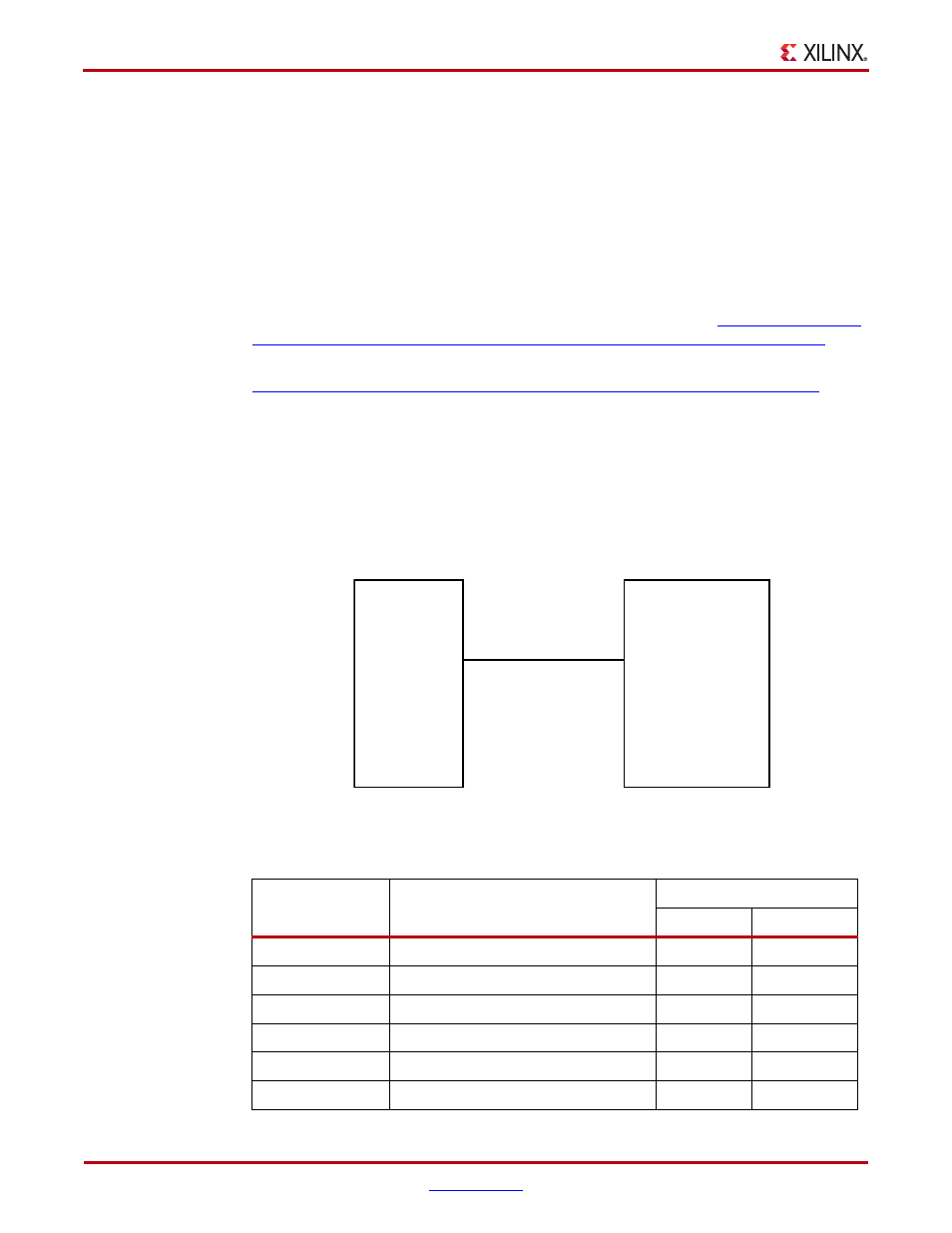
Figure 1-9:
Linear Flash BPI Interface
Table 1-7:
BPI Memory Connections
FPGA U1 Pin
Schematic Netname
BPI Memory U10
Pin Number
Pin
K18
FLASH_A0
32
A0
K17
FLASH_A1
28
A1
J18
FLASH_A2
27
A2
J16
FLASH_A3
26
A3
G18
FLASH_A4
25
A4
G16
FLASH_A5
24
A5
U1
U10
FPGA
BPI FLASH
INTERFACE
NUMONYX TYPE J3vD
T28F128J3D-75
ADDR, DATA, CTRL
UG518_09_070809