Spartan-6 xc6slx16-2csg324 fpga, Configuration, I/o voltage rails – Xilinx SP601 Hardware UG518 User Manual
Page 13
SP601 Hardware User Guide
13
UG518 (v1.1) August 19, 2009
Detailed Description
1. Spartan-6 XC6SLX16-2CSG324 FPGA
A Xilinx Spartan-6 XC6SLX16-2CSG324 FPGA is installed on the Embedded Development
Board.
Configuration
The SP601 supports configuration in the following modes:
•
Master SPI x4
•
Master SPI x4 with off-board device
•
BPI
•
JTAG (using the included USB-A to Mini-B cable)
For details on configuring the FPGA, see
I/O Voltage Rails
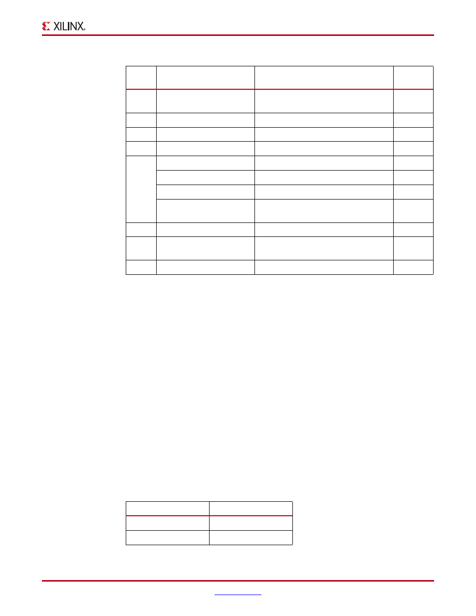
There are four available banks on the LX16-CS324 device. Banks 0, 1, and 2 are connected
for 2.5V I/O. Bank 3 is used for the 1.8V DDR2 component memory interface of Spartan-6
FPGA’s hard memory controller. The voltage applied to the FPGA I/O banks used by the
SP601 board is summarized in
Table 1-2
.
9
VITA 57.1 FMC-LPC
connector
LVDS signals, clocks, PRSNT
6
10
LEDs
Ethernet PHY Status
7
11
LED, Header
FPGA Awake LED, Suspend Header
8
12
LEDs
FPGA INIT, DONE
9
13
LED
User I/O (active-High)
9
DIP Switch
User I/O (active-High)
9
Pushbutton
User I/O, CPU_RESET (active-High)
9
12-pin (8 I/O) Header
6 pins x 2 male header with 8 I/Os
(active-High)
10
14
Pushbutton
FPGA_PROG_B
9
15
USB JTAG
Cypress USB to JTAG download cable
logic
14, 15
16
Onboard Power
Power Management
11,12,13
Table 1-1:
SP601 Features (Cont’d)
Number
Feature
Notes
Schematic
Page
Table 1-2:
I/O Voltage Rail of FPGA Banks
FPGA Bank
I/O Voltage Rail
0
2.5V
1
2.5V