2 interrupt timing – Texas Instruments TMS3320C5515 User Manual
Page 55
www.ti.com
Interrupts
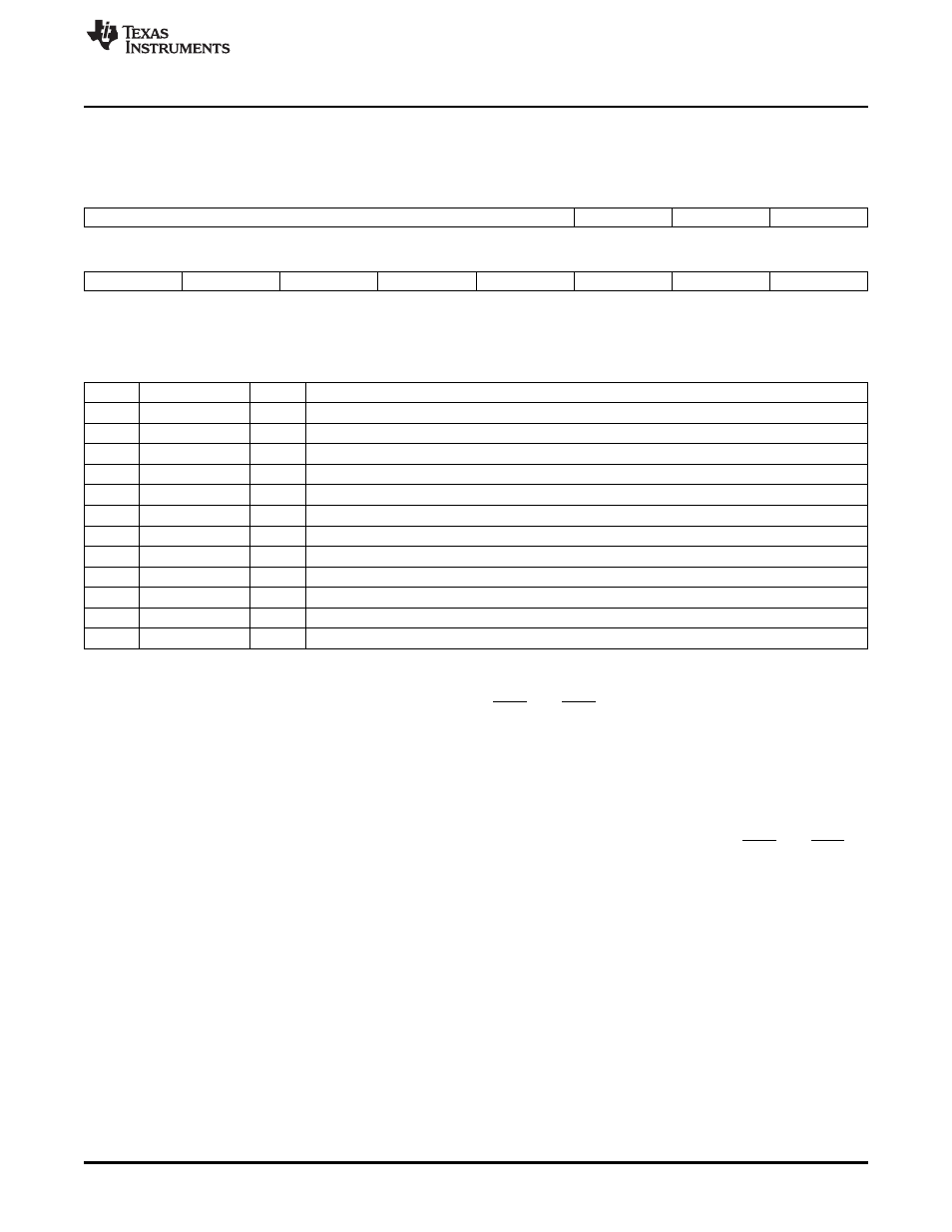
The interrupt flag register (IFR1) and interrupt enable register 1 (IER1) bit layouts are shown in
and described in
.
Figure 1-26. IFR1 and IER1 Bit Locations
15
11
10
9
8
Reserved
RTOS
DLOG
BERR
R-0
R/W-0
R/W-0
R/W-0
7
6
5
4
3
2
1
0
I2C
EMIF
GPIO
USB
SPI
RTC
RCV3
XMT3
R/W-0
R/W-0
R/W-0
R/W-0
R/W-0
R/W-0
R/W-0
R/W-0
LEGEND: R/W = Read/Write; R = Read only; -n = value after reset
Table 1-34. IFR1 and IER1 Bit Descriptions
Bit
Field
Value
Description
15-11
Reserved
0
Reserved. This bit should always be written with 0.
10
RTOS
1-0
Real-Time operating system interrupt flag/mask bit.
9
DLOG
1-0
Data log interrupt flag/mask bit.
8
BERR
1-0
Bus error interrupt flag/mask bit.
7
I2C
1-0
I2C interrupt flag/mask bit.
6
EMIF
1-0
EMIF error interrupt flag/mask bit.
5
GPIO
1-0
GPIO aggregated interrupt flag/mask bit.
4
USB
1-0
USB interrupt flag/mask bit.
3
SPI
1-0
SPI interrupt flag/mask bit.
2
RTC
1-0
Wakeup or real-time clock interrupt flag/mask bit.
1
RCV3
1-0
I2S3 receive interrupt flag/mask bit.
0
XMT3
1-0
I2S3 transmit interrupt flag/mask bit.
1.6.2 Interrupt Timing
The interrupt signals on the external interrupts pins (INT0 and INT1) are detected with a synchronous
negative edge detector circuit. To reliably detect the external interrupts, the interrupt signal must have at
least 2 SYSCLK high followed by at least 2 SYSCLK low.
To define the minimum low pulse width in nanoseconds scale, you should take into account that the
on-chip PLL of the device is software programmable and that your application may be dynamically
changing the frequency of PLL. You should use the slowest frequency that will be used by your application
to calculate the minimum interrupt pulse duration in nanoseconds.
When the system master clock is disabled (SYSCLKDIS =1), the external interrupt pins (INT0 and INT1)
will be asynchronously latched and held low while the clocks are re-enabled. Once the clocks are
re-enabled, the DSP will latch the interrupt in the IFR.
55
SPRUFX5A – October 2010 – Revised November 2010
System Control
Copyright © 2010, Texas Instruments Incorporated