Texas Instruments TMS320 User Manual
Adv ance informa t ion, Tms320 second generation digital signal processors

TMS320 SECOND GENERATION
DIGITAL SIGNAL PROCESSORS
SPRS010B — MAY 1987 — REVISED NOVEMBER 1990
POST OFFICE BOX 1443
HOUSTON, TEXAS 77001
1
ADVANCE INFORMATION concerns new products in the
sampling or preproduction phase of development.
Characteristic data and other specifications are subject to
change without notice.
Copyright
1991, Texas Instruments Incorporated
80-ns Instruction Cycle Time
544 Words of On-Chip Data RAM
4K Words of On-Chip Secure Program
EPROM (TMS320E25)
4K Words of On-Chip Program ROM
(TMS320C25)
128K Words of Data/Program Space
32-Bit ALU/Accumulator
16 16-Bit Multiplier With a 32-Bit Product
Block Moves for Data/Program
Management
Repeat Instructions for Efficient Use of
Program Space
Serial Port for Direct Codec Interface
Synchronization Input for Synchronous
Multiprocessor Configurations
Wait States for Communication to Slow
Off-Chip Memories/Peripherals
On-Chip Timer for Control Operations
Single 5-V Supply
Packaging: 68-Pin PGA, PLCC, and
CER-QUAD
68-to-28 Pin Conversion Adapter Socket for
EPROM Programming
Commercial and Military Versions Available
NMOS Technology:
— TMS32020
200-ns cycle time
. . . . . . . . .
CMOS Technology:
— TMS320C25
100-ns cycle time
. . . . . . . .
— TMS320E25
100-ns cycle time
. . . . . . . .
— TMS320C25-50
80-ns cycle time
. . . . . .
description
This data sheet provides complete design documentation for the second-generation devices of the TMS320
family. This facilitates the selection of the devices best suited for user applications by providing all specifications
and special features for each TMS320 member. This data sheet is divided into four major sections: architecture,
electrical specifications (NMOS and CMOS), timing diagrams, and mechanical data. In each of these sections,
generic information is presented first, followed by specific device information. An index is provided for quick
reference to specific information about a device.
1 2 3 4 5 6 7 8 9 10 11
A
B
C
D
E
F
G
H
J
K
L
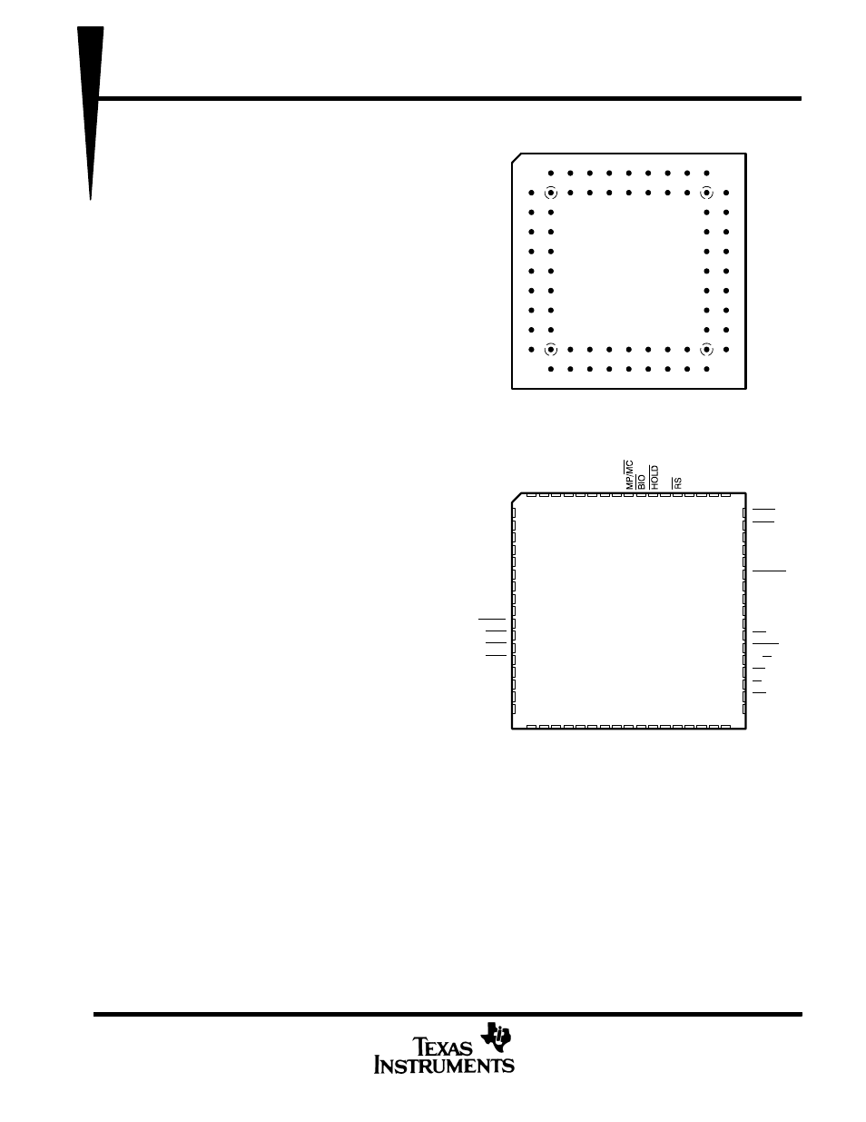
68-Pin GB Package
†
(Top View)
IACK
MSC
CLKOUT1
CLKOUT2
XF
HOLDA
DX
FSX
X2 CLKIN
X1
BR
D8
D9
D10
D1
1
D12
D13
D14
D15
READY
CLKR
CLKX
STRB
R/W
PS
IS
DS
V
SS
10
11
12
13
14
15
16
17
18
19
20
21
22
23
24
25
26
27 28 29 30 31 32 33 34 35 36 37 38 39 40 41 42 43
9 8 7 6 5 4 3 2 1 68 67 66 65 64 63 62 61
V
SS
D7
D6
D5
D4
D3
D2
D1
D0
SYNC
INT0
INT1
INT2
V
CC
DR
FSR
A0
60
59
58
57
56
55
54
53
52
51
50
49
48
47
46
45
44
A1
A2
A3
A4
A5
A6
A7
A8
A9
A10
A1
1
A12
A13
A14
A15
V
SS
V
CC
V
CC
V
CC
68-Pin FN and FZ Packages
†
(Top View)
ADV
ANCE
INFORMA
T
ION
