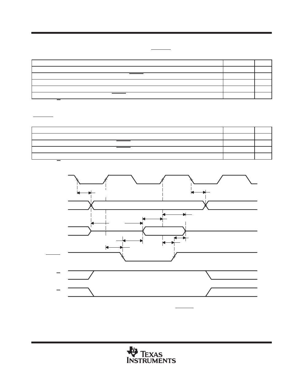
See figure 15) – Texas Instruments TMS320VC5402 User Manual
Page 43

TMS320VC5402
FIXEDĆPOINT DIGITAL SIGNAL PROCESSOR
SPRS079E – OCTOBER 1998 – REVISED AUGUST 2000
43
POST OFFICE BOX 1443
•
HOUSTON, TEXAS 77251–1443
memory and parallel I/O interface timing (continued)
timing requirements for a
parallel I/O port read (IOSTRB = 0) [H = 0.5 t
c(CO)
]
†
(see Figure 15)
MIN
MAX
UNIT
ta(A)IO
Access time, read data access from address valid
3H–7
ns
ta(ISTRBL)IO
Access time, read data access from IOSTRB low
2H–7
ns
tsu(D)IOR
Setup time, read data before CLKOUT high
6
ns
th(D)IOR
Hold time, read data after CLKOUT high
0
ns
th(ISTRBH-D)R
Hold time, read data after IOSTRB high
0
ns
† Address and IS timings are included in timings referenced as address.
switching characteristics over recommended operating conditions for a
parallel I/O port read
(IOSTRB = 0)
†
(see Figure 15)
PARAMETER
MIN
MAX
UNIT
td(CLKL-A)
Delay time, CLKOUT low to address valid
–2
3
ns
td(CLKH-ISTRBL)
Delay time, CLKOUT high to IOSTRB low
–2
3
ns
td(CLKH-ISTRBH)
Delay time, CLKOUT high to IOSTRB high
–2
3
ns
th(A)IOR
Hold time, address after CLKOUT low
0
3
ns
† Address and IS timings are included in timings referenced as address.
IS
R/W
IOSTRB
D[15:0]
A[19:0]
CLKOUT
th(A)IOR
td(CLKH-ISTRBH)
th(D)IOR
tsu(D)IOR
ta(A)IO
td(CLKH-ISTRBL)
td(CLKL-A)
ta(ISTRBL)IO
th(ISTRBH-D)R
NOTE A: A[19:16] are always driven low during accesses to I/O space.
Figure 15. Parallel I/O Port Read (IOSTRB = 0)
