3 reset, Table 35. typical power-down timings, Figure 16. reset block diagram – Intel SE8500HW4 User Manual
Page 72
Electrical Specifications
Intel® Server Board Set SE8500HW4
Revision
1.0
Intel order number D22893-001
60
Table 35. Typical Power-Down Timings
Ref
Description
Max
Typical
Min
t1
Time from front-panel power button push, to BMC asserting the power button to the
chipset. BMC debounces the power button input for 50ms
1s 90ms 50ms
t2
Time from BMC asserting power button to chipset, until chipset responds with
SLP_S5_L. Dependent on chipset setup.
5s 4.5s –
t3
Time from when SLP_S5_L is asserted, to when BMC deasserts PS_ON_L to
complete system power-off.
1s 160ms
50ms
t4
Time from BMC deasserting D2D enable, to when it deasserts PS_ON_L to
complete system power-off.
– 100µs
0µs
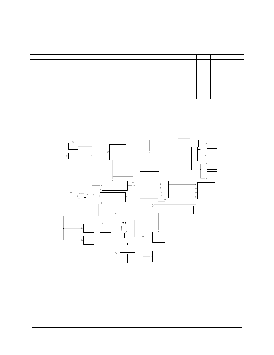
8.3 Reset
Figure 16 and Table 36 illustrate the reset routing in the Intel
®
Server Board Set SE8500HW4.
VID_PCI_RST_N
XDP1
XDP2
ICH5
NB
RESET BUTTON
FWH1
FWH2
SIO
PLD 1
PLD 3
PLD 1
Proc1
Proc2
Proc3
Proc4
PB1_RESET_N
PB0_RESET_N
IMI CONN 1
IMI CONN 2
IMI CONN 3
IMI CONN 4
IMI Hot
pl
ug
IMI_A_ISO_RST_N
IMI_B_ISO_RST_N
IMI_C_ISO_RST_N
IMI_D_ISO_RST_N
Power
Connector
PS1_PWROK
LEVEL
TRANSLATOR
OR
GATE
PB1_RESET
PB0_RESET
IM
I_A_RS
T
_N
IM
I_D_R
S
T
_N
IM
I_B_RST_N
IM
I_C_RST_N
IMI
NB_RESETI_N
ITP_DBR_RESET_N
FP_RST_BTN_N
LPC_FWH_LRESET_N
LP
C
_S
IO_
LR
ES
ET
_N
S
IO_
VI
D_
RST
Front Panel
Connector
Video
PC
I_
ID
E
_R
S
T
_N
PXH
IOP332
PX
H_
RES
E
T
I_
N
IO
P
332_
R
E
S
E
T
I_
N
NB
_R
_R
E
S
E
T
I_
N
PC
I_R
E
S
E
T
_N
IC
H5
_S
YS
_R
ST
_N
ITP_CPU_RESET_N
BUFFER
PCI_RST_BUFF1_N
SI
O_N
IC_
RS
T
PS2_PWROK
Network
PX2B_RST_N
N
IC_
RS
T_
N
Figure 16. Reset Block Diagram