7 jtag interface ac timing, 1 jtag interface ac timing table, 2 jtag interface test circuit – Marvel Group Integrated Controller 88F6281 User Manual
Page 101: Table 54, Jtag interface ac timing table, Figure 21, Jtag interface test circuit
Electrical Specifications
AC Electrical Specifications
Copyright © 2008 Marvell
Doc. No. MV-S104859-U0 Rev. E
December 2, 2008, Preliminary
Document Classification: Proprietary Information
Page 101
8.6.7
JTAG Interface AC Timing
8.6.7.1
JTAG Interface AC Timing Table
Table 54: JTAG Interface AC Timing Table
8.6.7.2
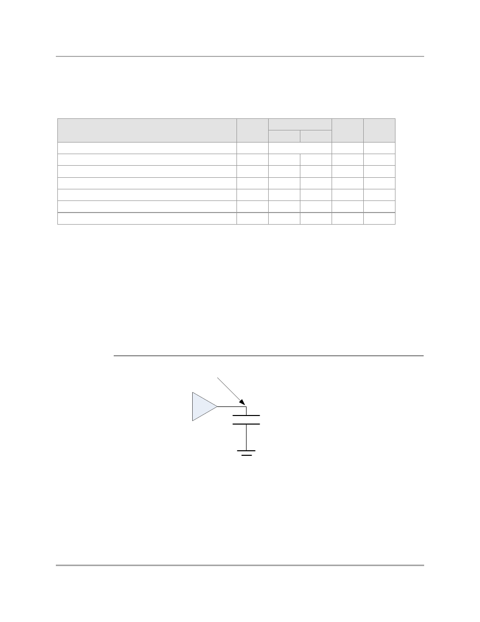
JTAG Interface Test Circuit
Figure 21: JTAG Interface Test Circuit
Min
Max
JTClk frequency
fCK
MHz
-
JTClk minimum pulse w idth
Tpw
0.45
0.55
tCK
-
JTClk rise/fall slew rate
Sr/Sf
0.50
-
V/ns
2
JTRSTn active time
Trst
1.0
-
ms
-
TMS, TDI input setup relative to JTClk rising edge
Tsetup
6.67
-
ns
-
TMS, TDI input hold relative to JTClk rising edge
Thold
13.0
-
ns
-
JTClk falling edge to TDO output delay
Tprop
1.0
8.33
ns
1
Notes:
General comment: All values w ere measured from vddio/2 to vddio/2, unless otherw ise specified.
General comment: tCK = 1/fCK.
1. For TDO signal, the load is CL = 10 pF.
2. Defined from VIL to VIH for rise time, and from VIH to VIL for fall time.
30.0
Notes
30 MHz
Description
Sym bol
Units
CL
Test Point