Freescale Semiconductor i.MX27 PDK 1.0 User Manual
Page 28
Freescale Semiconductor
i.MX27 PDK 1.0 Hardware User's Guide, Rev. 1.0
4-3
4.2 3-Stack Memory Map
Table 4-1 describes the memory map for the 3-Stack system. None of the memories take up the
entire address space of the associated chip selects, and the software can access the same physical
memory location at more than one range of address. For instance, DDR SDRAM occupies only
128 MB of the 256MB space available to CSD0, so it appears in two different ranges of
addresses.
Table 4-1 Memory Map
Peripheral
Chip Select
Address Range (HEX)
Size
DDR
¯¯¯¯¯¯¯¯¯¯¯¯
CSDO (CS2)
0x8000_0000 to 8FFF_FFFF
128MB
Ethernet Controller
LAN9217
¯¯¯¯
CS5
0xB600_0000 to B600_007F
128MB
External
UART-A DB9-Male
¯¯¯¯¯¯¯¯¯¯¯¯
CSDO (CS2)
0xB600_8000_ B600_8007
8 Bytes
W
E
IM
M
e
m
o
ry
B
u
s
16
bi
t
W
a
ll-
DC
-
In
GP
IO
S
E
RI
A
L
UA
RT
Lattice
1.8V/3.3V CPLD
SMSC
LAN 9217
100BT
WEIM BUS 3.3V
1.8V
DUART
XR16L570
Config
Switches
-buttons
LED’s
JTAG
RJ45
Connector
DB9
D
ebug-D
C
-
In
Interrupt
Button
Power
Select
Debug
Power
Supply
Debug Board
Power 3.3V
On/Off
Button
Aux
Power
Ethernet
XFMR
JT
A
G
DB9
Code-Test
Interface
2x Mictor
Data-Logger
Current
Monitoring
C
u
rre
nt
-S
ens
e
BootStrap
Reset
Button
DC
MAX3232
XCVR
MAX3232
XCVR
500 pin Connector
10x50
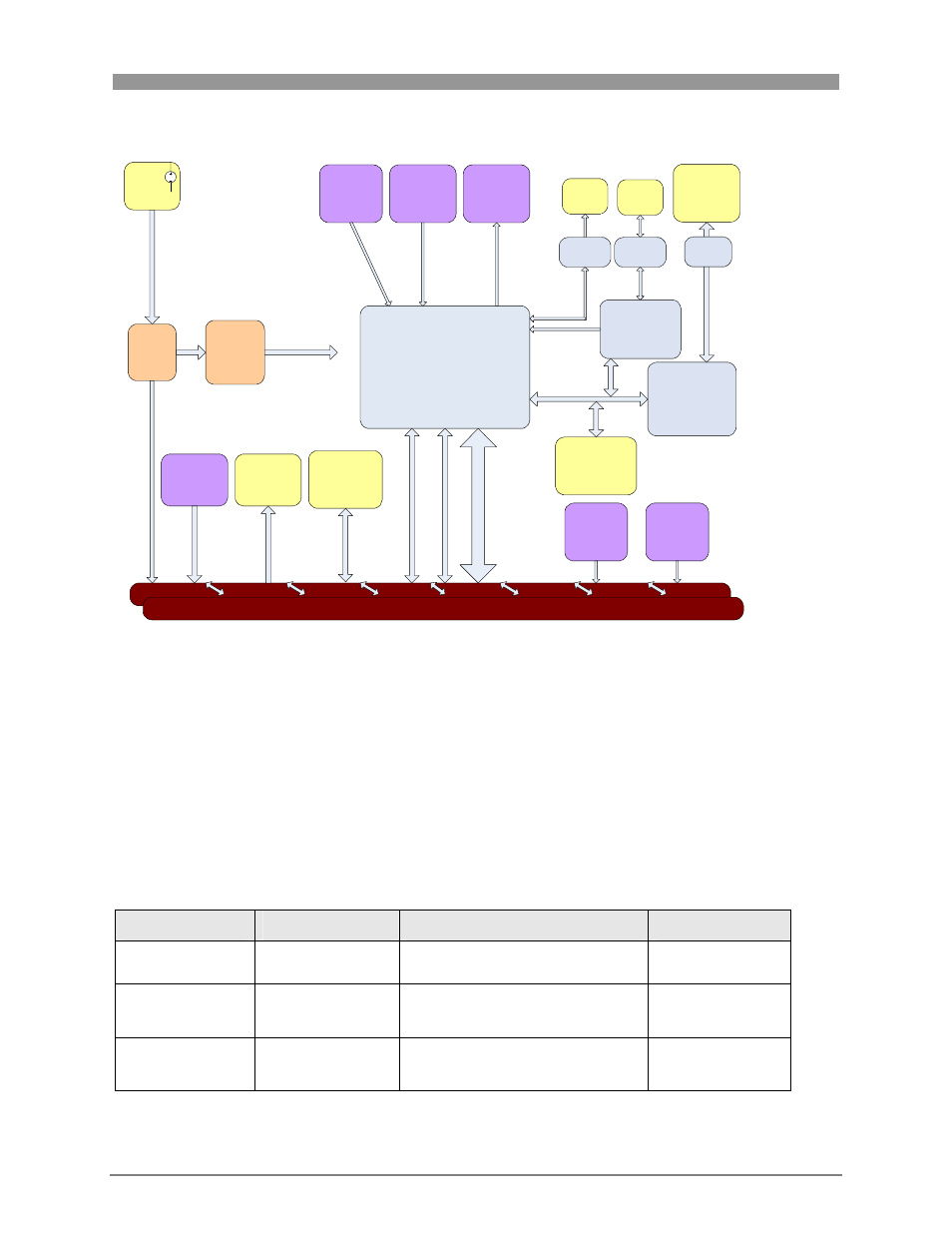
Figure 4-3 Functional Block 3 of 3