Epson Multi-mode Data Controller MFJ-1278B User Manual
Page 356
MFJ-1278B MULTI-MODE APPENDIX G: JUMPER FUNCTIONS
JUMPER FUNCTIONS AND LOCATIONS
The MFJ-1278B mother board has many jumper connectors. Each jumper connector has a
special function. The Jumper Function chart, Table G-1 in this appendix, will help in
identifying each jumper function. Figure G-1 will help in locating the jumper connectors
easily.
For normal operation a shorting jumper must be placed on the following connectors: JMP 5;
JMP 8; JMP 9 pins 2,3; JMP 13; JMP 14 pins 1,2; JMP 16 pins 1,3 and pins 2,4; JMP 18
pins 1,2; JMP 19 outside pair (one top,one bottom); JMP 22 pins 2,3; JMP 24 pins 1,2; JMP
26 pins 1,,2; JMP E, F, G, H. Also on the mode disconnect header J4 the following pins need
jumpers pins 1,2 11,12 13,14 17,18.
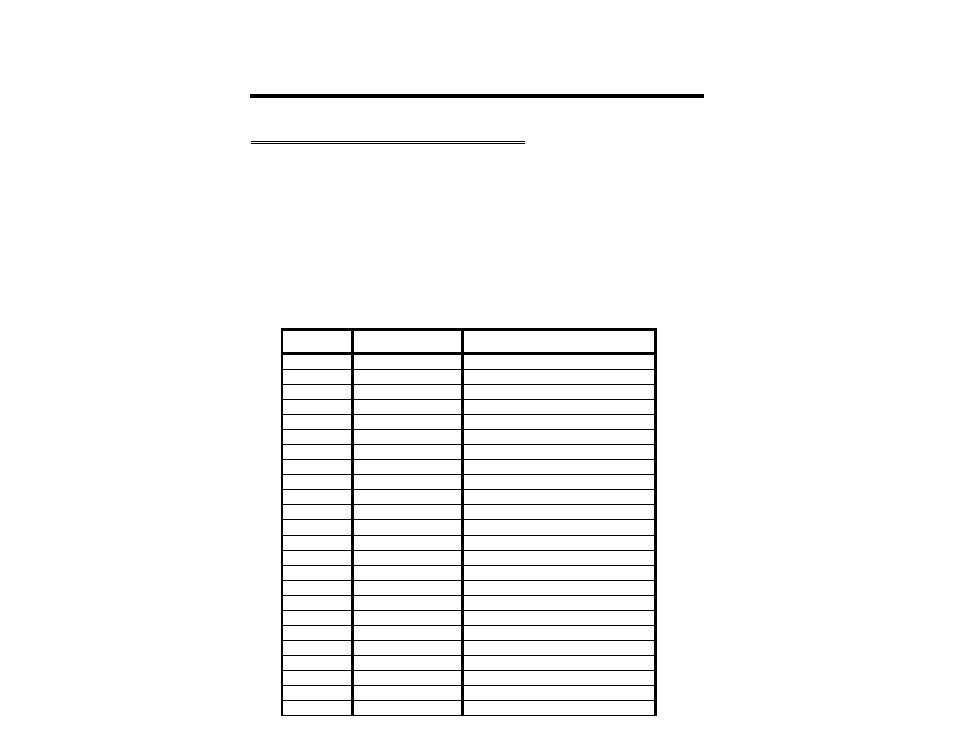
Table G-1: Jumper Function
Jumper #
Position
Function
JMP1
Pin 1 & 2
!DCD (RS-232C) stays on
Pin 2 & 3
!DCD (RS-232C) stays off
OFF (Default)
!DCD reflects connect status
JMP2
Pin 1 & 2 (Default)
4.92 MHz CPU clock
Pin 2 & 3
2.46 MHz CPU clock
JMP4
ON
Disable Tx watch-dog
OFF (Default)
Enable Tx watch-dog
JMP5
ON (Default)
Lithium battery connected
OFF
Lithium battery disconnected
JMP7
ON
Analog loopback mode
OFF (Default)
Normal modem operation
JMP8
ON (Default)
Demodulator enabled
OFF
Demodulator calibrate
JMP9
Pin 1 & 2
Calibrate U16 tones
Pin 2 & 3 (Default)
Normal modem operation
JMP10
ON
Digital loopback mode
OFF (Default)
Normal modem operation
JMP11
LEFT
Transmit data NRZ
RIGHT (Default)
Transmit data NRZI
JMP13
ON (Default)
TTL, RTS enable
OFF
TTL, RTS disable
JMP14
Pin 1 & 2 (Default)
FSK out normal
Pin 2 & 3
FSK out reverse
JMP16
Pin 1 & 2
Without multi-gray levels