Motor control applications, Charges up (through d, Hv+ - [hv- + v – Avago Technologies ACPL-224-500E User Manual
Page 50: Is the voltage across diode d, And hv+, hv- are the rail voltages, Pulls up to hv+ -v, This causes c, Charge sharing be- tween c, And c, Results in the voltage across c
AV02-4387EN
47
Avago Technologies
16
15
14
13
12
11
10
9
1
2
3
4
5
6
7
8
VIN+
VIN–
V
CC1
GND1
RESET
FAULT
VLED1+
VLED1–
VE
VLED2+
DESAT
V
CC2
VC
VOUT
V
EE
V
EE
HIGH GATE-DRIVE
(LOW GATE-DRIVE CIRCUIT IS
IDENTICAL TO HIGH
GATE-DRIVE CIRCUIT)
HCPL-316J
16
15
14
13
12
11
10
9
1
2
3
4
5
6
7
8
VIN+
VIN–
V
CC1
GND1
RESET
FAULT
VLED1+
VLED1–
VE
VLED2+
DESAT
V
CC2
VC
VOUT
V
EE
V
EE
LOW GATE-DRIVE
HCPL-316J
N/C
R
TONH
10
R
BIASDH
20K
V
CC2
(H)
V
DESAT
(H)
V
C
(H)
V
O
(H)
V
E
(H)
V
EE
(H)
D
ZLH
18 V
C
2H
1.2
µF
(20%)
C
3H
0.1
µF
1 k
R
DESATH
R
GH
12.5
D
Z2H
12 V
C
4H
250 nF
D
2H
A14P
1,000 V
R
1L
47K
R
2L
20
15nF
C
1L
1K
R
DESATL
D
DSL
HV DIODE
R
GL
12.5
D
FBLO
(DSE130-12A,
IXYS)
HV–
AC
MOTOR
D
FBHI
(DSE130-12A,
IXYS)
D
DSH
A14P
1,000 V
HV+
DUAL IGBT
R
2H
20
15 nF
C
1H
HV+
HV+
R
1H
47K
D
1H
A14P
1,000 V
M1
M2
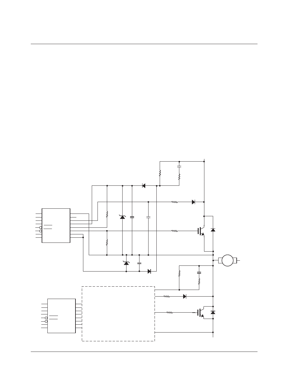
Figure 4. Bootstrap Circuit for Power Control System
Motor Control Applications
Figure 4 shows a bootstrapped out-
put power supply circuit that has
the following benefits:
• eliminates the need for an iso-
lated power supply or a dc-to-dc
converter,
• lower cost solution compared to
transformer based power supply,
• less printed circuit board space.
This circuit includes a bootstrap
circuit for providing output power
to the HCPL-316J gate drive opto-
couplers, thereby eliminating the
need for isolated power supplies or
dc-to-dc converters. It can be modi-
fied to suit other Avago gate drive
optocouplers and current/voltage
sensing isolation amplifiers.
Component values were chosen for
a 350 V rail =
HV+ - HV - (240 V x 1.414).
When the lower IGBT is turned on,
V
C1H
charges up (through
D
1H
) to a voltage of:
V
C1H
= HV+ - [HV- + V
SATM2
+ V
CC2H
+
V
F
(D
1H
)]
= 350 V - 3 V - 18 V - 1 V
= 328 V
where V
SATM2
is the saturation or
“on” voltage across the collector-
emitter of IGBT M2; V
F (D1H)
is the
voltage across diode D
D1H
; and
HV+, HV- are the rail voltages.
Bootstrap Power Supply Circuit for Power Control Systems
When M2 (low IGBT) switches off
and M1 (upper IGBT) switches on,
V
E(H)
pulls up to HV+ -V
SATM1
. This
causes C
4H
to become charged
through D
2H
. Charge sharing be-
tween C
1H
and C
4H
results in the voltage across C
4H
which (in the absence of clamping
diode D
Z2H
) can be approximated
by:
C
4H
× ∆V
C4H
= C
1H
× 328 V
->
∆V
C4H
= 19.6 V
where
∆V
C4H
= the voltage drop
across C
4H
. The negative gate bias
then is held at 12 V by clamping
Zener D
Z2H
.
- ACPL-227-500E ACPL-244-500E ACPL-247-500E ACPL-785J-000E ACPL-C780-000E ACPL-C784-000E ACPL-C78A-000E HCPL-0201 HCPL-0211 HCPL-0300 HCPL-0302 HCPL-0314 HCPL-0370 HCPL-0452 HCPL-0453 HCPL-0454 HCPL-0466 HCPL-0500 HCPL-0501 HCPL-050L HCPL-0530 HCPL-0531 HCPL-0534 HCPL-053L HCPL-0600 HCPL-0601 HCPL-060L HCPL-0611 HCPL-061A HCPL-061N HCPL-0630 HCPL-0631 HCPL-063A HCPL-063L HCPL-063N HCPL-0661 HCPL-0700 HCPL-0701 HCPL-0708 HCPL-070A HCPL-070L HCPL-0710 HCPL-0720 HCPL-0721 HCPL-0723 HCPL-0730 HCPL-0731 HCPL-0738 HCPL-073A HCPL-073L HCPL-0872 HCPL-0900 HCPL-090J HCPL-091J HCPL-092J HCPL-0930 HCPL-0931 HCPL-177K HCPL-177k#200 HCPL-177K-100 HCPL-177K-300 HCPL-177K-600 HCPL-181-000E HCPL-1930 HCPL-1930#100 HCPL-1930#200 HCPL-1930#300 HCPL-1931 HCPL-1931#100 HCPL-1931#200 HCPL-1931#300 HCPL-193K HCPL-193K#200 HCPL-2200 HCPL-2201 HCPL-2202 HCPL-2211 HCPL-2212 HCPL-2219 HCPL-2231 HCPL-2232 HCPL-2300 HCPL-2400 HCPL-2430 HCPL-2502 HCPL-2503 HCPL-250L HCPL-2530 HCPL-2531 HCPL-2533 HCPL-253L HCPL-257K HCPL-257K#200 HCPL-257K-100 HCPL-257K-300 HCPL-2601 HCPL-2602 HCPL-260L HCPL-2611 HCPL-2612 HCPL-261A HCPL-261N HCPL-2630 HCPL-2631 HCPL-263A HCPL-263L HCPL-263N HCPL-268K HCPL-268K#200 HCPL-268K-100 HCPL-268K-300 HCPL-270L HCPL-2730 HCPL-2731 HCPL-273L HCPL-3020 HCPL-3120 HCPL-3140 HCPL-314J HCPL-3150 HCPL-315J HCPL-316J HCPL-3180 HCPL-354-000E HCPL-3700 HCPL-3760 HCPL-4100 HCPL-4200 HCPL-4502 HCPL-4503 HCPL-4504 HCPL-4506 HCPL-4534 HCPL-4562 HCPL-4661 HCPL-4701 HCPL-4731 HCPL-5120 HCPL-5120-100 HCPL-5120-200 HCPL-5120-300 HCPL-5121 HCPL-5121-100 HCPL-5121-200 HCPL-5121-300 HCPL-5150 HCPL-5150-100 HCPL-5150-200 HCPL-5150-300 HCPL-5151 HCPL-5151-100 HCPL-5151-200 HCPL-5151-300 HCPL-5200 HCPL-5200#100 HCPL-5200#200 HCPL-5200#300 HCPL-5201 HCPL-5201#100 HCPL-5201#200 HCPL-5201#300 HCPL-520K HCPL-520K#200 HCPL-520K-100 HCPL-520K-300 HCPL-5230 HCPL-5230#100 HCPL-5230#200 HCPL-5230#300 HCPL-5231 HCPL-5231#100 HCPL-5231#200 HCPL-5231#300 HCPL-523K HCPL-523K#200 HCPL-523K-100 HCPL-523K-300 HCPL-5300 HCPL-5300#100 HCPL-5300#200 HCPL-5300#300 HCPL-5301 HCPL-5301#100 HCPL-5301#200 HCPL-5301#300 HCPL-530K HCPL-530K#200 HCPL-5400 HCPL-54#100 HCPL-54#200 HCPL-54#300 HCPL-5401 HCPL-5401#100 HCPL-5401#200 HCPL-5401#300 HCPL-540K HCPL-540K#200 HCPL-540K-100 HCPL-540K-300 HCPL-5430 HCPL-5430#100 HCPL-5430#200 HCPL-5430#300 HCPL-5431 HCPL-5431#100 HCPL-5431#200 HCPL-5431#300 HCPL-543K HCPL-543K#200 HCPL-543K-100 HCPL-543K-300 HCPL-5500 HCPL-5500#100 HCPL-5500#200 HCPL-5500#300 HCPL-5501 HCPL-5501#100 HCPL-5501#200 HCPL-5501#300 HCPL-550K HCPL-550K#200 HCPL-550K-100 HCPL-550K-300 HCPL-5530 HCPL-5530#100 HCPL-5530#200 HCPL-5530#300 HCPL-5531 HCPL-5531#100 HCPL-5531#200 HCPL-5531#300 HCPL-553K HCPL-553K#200 HCPL-553K#300 HCPL-553K-100 HCPL-5600 HCPL-5600#100 HCPL-5600#200 HCPL-5600#300 HCPL-5601 HCPL-5601#100 HCPL-5601#200 HCPL-5601#300 HCPL-560K HCPL-560K#200 HCPL-560K-300 HCPL-560K-100 HCPL-5630 HCPL-5630#100 HCPL-5630#200 HCPL-5630#300 HCPL-5631 HCPL-5631#100 HCPL-5631#200 HCPL-5631#300 HCPL-563K HCPL-563K#200 HCPL-563K-100 HCPL-563K-300 HCPL-5650 HCPL-5650#200 HCPL-5651 HCPL-5651#200 HCPL-5700 HCPL-5700#100 HCPL-5700#200 HCPL-5700#300 HCPL-5701 HCPL-5701#100 HCPL-5701#200 HCPL-5701#300 HCPL-570K HCPL-570K#200 HCPL-570K#300 HCPL-570K-100 HCPL-5730 HCPL-5730#100 HCPL-5730#200 HCPL-5730#300 HCPL-5731 HCPL-5731#100 HCPL-5731#200 HCPL-5731#300 HCPL-573K HCPL-573K#200 HCPL-573K#300 HCPL-573K-100 HCPL-5760 HCPL-5760#100 HCPL-5760#200 HCPL-5760#300 HCPL-5761 HCPL-5761#100 HCPL-5761#200 HCPL-5761#300 HCPL-576K HCPL-576K#200 HCPL-576K-100 HCPL-6230 HCPL-6231 HCPL-623K HCPL-6250 HCPL-6251 HCPL-625K HCPL-6430 HCPL-6431 HCPL-643K HCPL-6530 HCPL-6531 HCPL-653K HCPL-6550 HCPL-6551 HCPL-655K HCPL-6630 HCPL-6631 HCPL-663K HCPL-6650 HCPL-6651 HCPL-665K HCPL-6730 HCPL-6731 HCPL-673K HCPL-6750 HCPL-6751 HCPL-675K HCPL-7510 HCPL-7520 HCPL-7560 HCPL-7710 HCPL-7720 HCPL-7721 HCPL-7723 HCPL-7800 HCPL-7800A HCPL-7840 HCPL-7850 HCPL-7850#100 HCPL-7850#200 HCPL-7850#300 HCPL-7851 HCPL-7851#100 HCPL-7851#200 HCPL-7851#300 HCPL-7860 HCPL-786J HCPL-788J HCPL-814-000E HCPL-817-000E HCPL-9000 HCPL-900J HCPL-901J HCPL-902J HCPL-9030 HCPL-9031 HCPL-J312 HCPL-J314 HCPL-J454 HCPL-J456 HCPL-M452 HCPL-M453 HCPL-M454 HCPL-M456 HCPL-M600 HCPL-M601 HCPL-M611 HCPL-M700 HCPL-M701 HCPL-T250 HCPL-T251