6 input dual opamp structure – Sundance SMT916 User Manual
Page 10
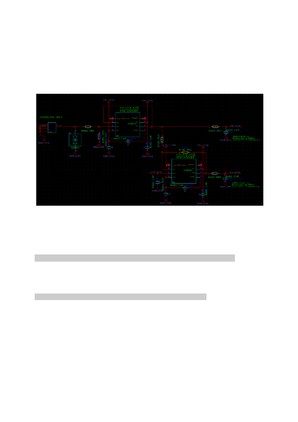
An AD8031 is used to route the common mode voltage from the ADC to the input
opamp.
3.3.2.6 Input dual opamp structure
The analogue input on the connector is single ended. Two opamps are used to
provide positive and negative differential lines to the ADC. Both are centred on the
common mode voltage to ensure maximum scale and linearity.
Figure 3 - ADCs input front-end.
AD8021 opamps are used as able to match 16-bit ADC converters inputs. They
receive symmetrical power supplies provided by LDOs belonging to the same family,
ensuring a better symmetry.
3.4 Firmware
The firmware shown below is what has been designed to be implemented in the
FPGA of an SMT372T.
3.4.1 FPGA Block Diagram.
The block diagram of the firmware is shown below. An Ethernet interface is used to
communicate with the DSP (dspa). Control registers are collected from there. Main
settings will be the enable channel bits to activate ADC channels individually, to set
the rate of the sampling frequency (also called conversion rate), to trigger storage
units and to program individual iodelay (one setting per ADC channel).
ADCs are configured into self-clock mode. The FPGA sends to each ADC (via clock
distribution chip) a clock that the converter uses to serialise samples out. In order
for the FPGA to latch serial data in, it needs to re-align internally an image of the
clock it sends to the converters with the incoming data. This is implemented using