4 register architecture 4.1 data transfers, 2 fifo data buffer, 3 control & data registers – Measurement Computing CIO-DAS16/330 User Manual
Page 12
4 REGISTER ARCHITECTURE
4.1 DATA TRANSFERS
The CIO-DAS16/330 bus interface is a PC/XT/AT bus interface. In compatibility mode (mode switch up) it interfaces to
the XT bus only. In enhanced mode (mode switch DOWN), the CIO-DAS16/330 employs the full 16-bit PC/AT bus.
Because 16-bit data transfers are faster, the CIO-DAS16/330 can transfer A/D samples taken with old DAS-16 software
at speeds over 150 kHz. Old DAS-16 software uses DMA to transfer A/D data.
Of course, using the REP INS command (which can only be done by the CIO-DAS16/330), data transfers of 330 kHz and
sample sets of any size up to the size of available memory may be taken.
4.2 FIFO DATA BUFFER
The First In First Out (FIFO) buffer is a specialized memory 1024 samples deep. After each conversion, the A/D data is
transferred to the FIFO memory. Samples are retrieved from the FIFO data buffer by the computer program which stores
the data in the PC's memory. This may be a language program, or an application program.
The FIFO is active all the time, regardless of mode. The FIFO does not affect compatibility with existing software, in
fact, it does enhance it by allowing data to be transferred asynchronously, therefore at higher speeds.
In addition to enhancing standard interrupt and DMA operations, the FIFO makes possible the use of advanced
instructions like REP-INSW, a block transfer.
4.3 CONTROL & DATA REGISTERS
The CIO-DAS16/330 is controlled and monitored by writing to and reading from 16 or 20 consecutive 8-bit I/O
addresses. The first address, or BASE ADDRESS, is determined by setting a bank of switches on the board.
Usually, register manipulation is best left to experienced programmers with a specific need for low level control as most
of the CIO-DAS16/330 possible functions are implemented in the easy to use Universal Library™ for DOS and Windows
languages.
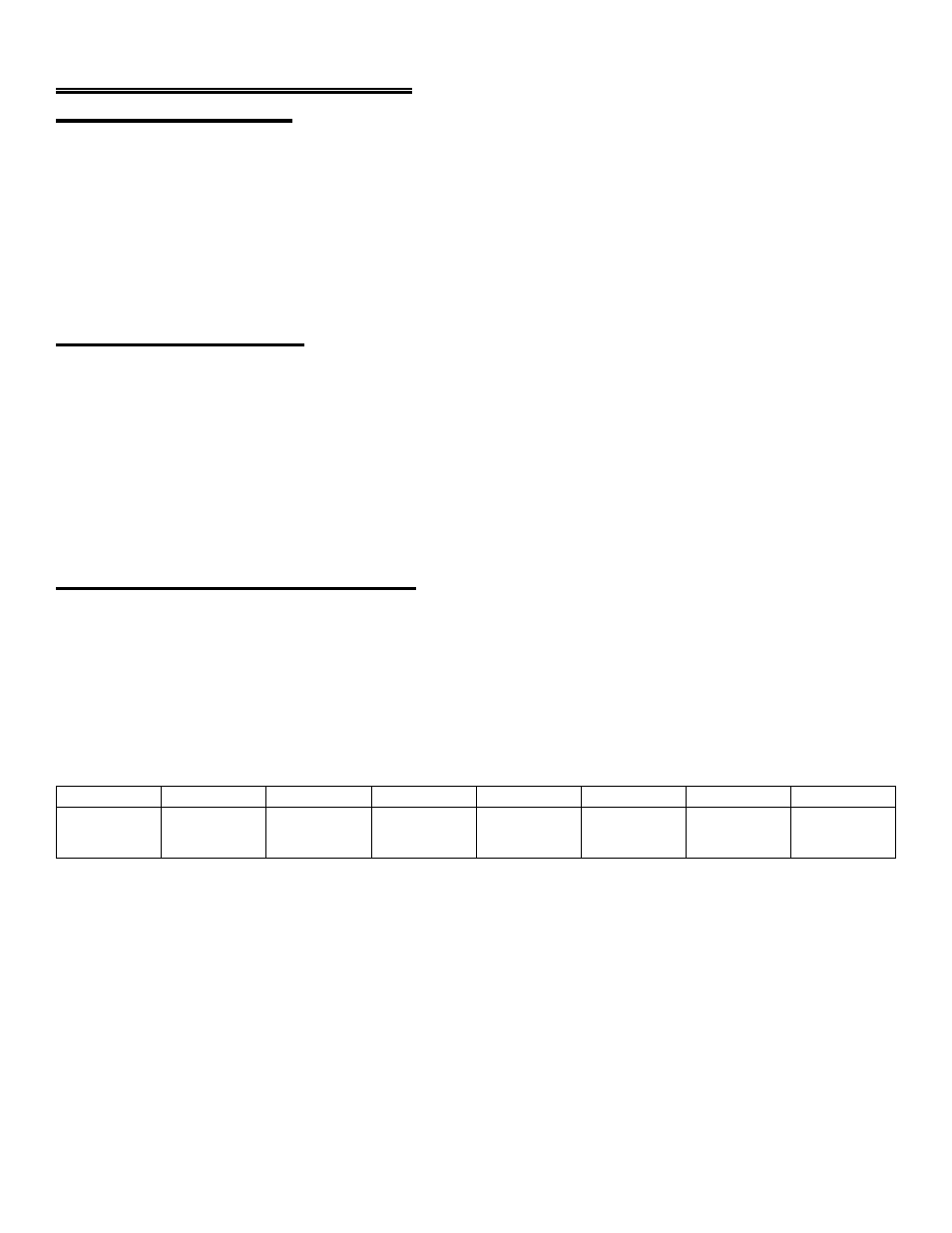
The register descriptions have the following format:
CH1
CH2
CH4
CH8
A/D12
LSB
A/D11
A/D10
A/D9
0
1
2
3
4
5
6
7
Where the numbers along the top row are the bit positions within the 8-bit byte and the numbers and symbols in the
bottom row are the functions associated with that bit.
To write to or read from a register in decimal or HEX, the weights in Table 4-1 apply.
8