Altera Cyclone V GX FPGA Development Board User Manual
Page 43
Chapter 2: Board Components
2–35
Memory
May 2013
Altera Corporation
Cyclone V GX FPGA Development Board
Reference Manual
C3
DDR3A_DQ9
AK16
1.5-V SSTL Class I
Data bus byte lane 1
A3
DDR3A_DQ10
AG17
1.5-V SSTL Class I
Data bus byte lane 1
D7
DDR3A_DQ11
AJ18
1.5-V SSTL Class I
Data bus byte lane 1
A2
DDR3A_DQ12
AG16
1.5-V SSTL Class I
Data bus byte lane 1
C2
DDR3A_DQ13
AF16
1.5-V SSTL Class I
Data bus byte lane 1
B8
DDR3A_DQ14
AJ19
1.5-V SSTL Class I
Data bus byte lane 1
C8
DDR3A_DQ15
AH20
1.5-V SSTL Class I
Data bus byte lane 1
F3
DDR3A_DQS_P0
Y16
Differential 1.5-V SSTL
Class I
Data strobe P byte lane 0
G3
DDR3A_DQS_N0
AA16
Differential 1.5-V SSTL
Class I
Data strobe N byte lane 0
C7
DDR3A_DQS_P1
Y17
Differential 1.5-V SSTL
Class I
Data strobe P byte lane 1
B7
DDR3A_DQS_N1
Y18
Differential 1.5-V SSTL
Class I
Data strobe N byte lane 1
K1
DDR3A_ODT
AH14
1.5-V SSTL Class I
On-die termination enable
J3
DDR3A_RASN
AG9
1.5-V SSTL Class I
Row address select
T2
DDR3A_RESETN
AK21
1.5-V SSTL Class I
Reset
L3
DDR3A_WEN
AK5
1.5-V SSTL Class I
Write enable
L8
DDR3A_ZQ01
—
1.5-V SSTL Class I
ZQ impedance calibration
DDR3 x16 (U22)
N3
DDR3A_A0
AJ12
1.5-V SSTL Class I
Address bus
P7
DDR3A_A1
AK12
1.5-V SSTL Class I
Address bus
P3
DDR3A_A2
AH11
1.5-V SSTL Class I
Address bus
N2
DDR3A_A3
AH12
1.5-V SSTL Class I
Address bus
P8
DDR3A_A4
AG13
1.5-V SSTL Class I
Address bus
P2
DDR3A_A5
AG14
1.5-V SSTL Class I
Address bus
R8
DDR3A_A6
AK10
1.5-V SSTL Class I
Address bus
R2
DDR3A_A7
AK11
1.5-V SSTL Class I
Address bus
T8
DDR3A_A8
AF11
1.5-V SSTL Class I
Address bus
R3
DDR3A_A9
AG11
1.5-V SSTL Class I
Address bus
L7
DDR3A_A10
AJ8
1.5-V SSTL Class I
Address bus
R7
DDR3A_A11
AK8
1.5-V SSTL Class I
Address bus
N7
DDR3A_A12
AJ7
1.5-V SSTL Class I
Address bus
T3
DDR3A_A13
AK7
1.5-V SSTL Class I
Address bus
M2
DDR3A_BA0
AH9
1.5-V SSTL Class I
Bank address bus
N8
DDR3A_BA1
AH10
1.5-V SSTL Class I
Bank address bus
M3
DDR3A_BA2
AJ10
1.5-V SSTL Class I
Bank address bus
K3
DDR3A_CASN
AF9
1.5-V SSTL Class I
Row address select
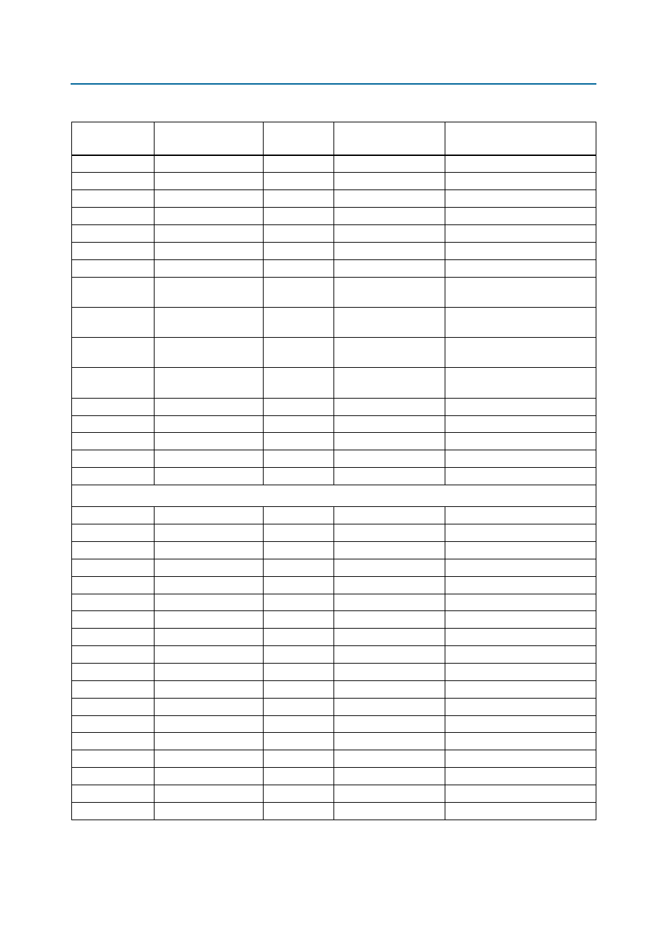
Table 2–29. DDR3A Device Pin Assignments, Schematic Signal Names, and Functions (Part 2 of 4)
Board Reference
Schematic
Signal Name
Cyclone V GX
Pin Number
I/O Standard
Description