Fpga programming over embedded usb-blaster, Fpga programming over embedded usb-blaster –11 – Altera Cyclone V GX FPGA Development Board User Manual
Page 19
Chapter 2: Board Components
2–11
FPGA Configuration
May 2013
Altera Corporation
Cyclone V GX FPGA Development Board
Reference Manual
FPGA Programming over Embedded USB-Blaster
This configuration method implements a USB type-B connector (J12), a USB 2.0 PHY
device (U16), and an Altera MAX II CPLD EPM240M100C4N (U20) to allow FPGA
configuration using a USB cable. This USB cable connects directly between the USB
type-B connector on the board and a USB port of a PC running the Quartus II
software.
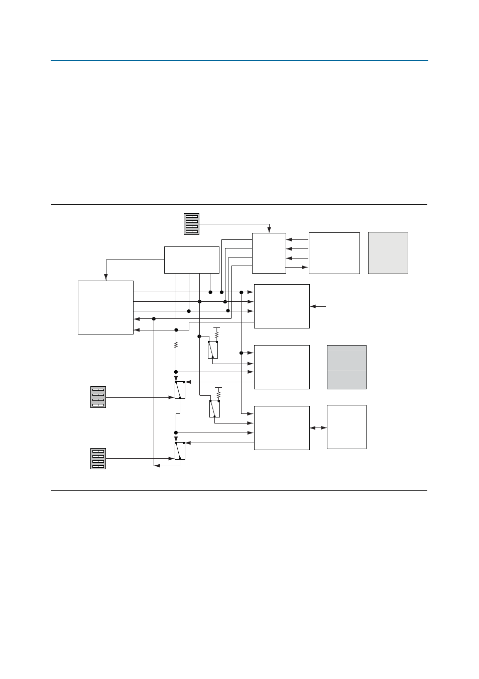
The embedded USB-Blaster in the MAX II CPLD EPM570F100C5N normally masters
the JTAG chain.
illustrates the JTAG chain.
The JTAG chain control DIP switch (SW5) controls the jumpers shown in
To connect a device or interface in the chain, their corresponding switch must be in
the OFF position. Slide all the switches in the ON position to only have the FPGA in
the chain.
1
The MAX V CPLD 5M2210 System Controller must be in the JTAG chain to use some
of the GUI interfaces.
Figure 2–3. JTAG Chain
Embedded
USB-Blaster II
GPIO
TCK
Cyclone V GX
FPGA
Analog
Switch
MAX V
System
Controller
HSMC
Port
GPIO
TMS
GPIO
TDO
GPIO
GPIO
TDI
JTAG Master
GPIO
Enable
Disable
Enable
Enable
JTAG Slave
HSMC
TCK
TMS
TDI
TDO
TCK
2.5 V
TMS
TDI
TDO
TCK
TMS
TDI
TDO
JTAG Slave
JTAG Slave
Analog
Switch
Always
Enabled
(in JTAG chain)
DIP Switch
DIP Switch
DIP Switch
10-pin
JTAG Header
Flash
Memory
PCI Express
Edge
Connector
JTAG Master
PCI Express
Motherboard
TCK
TMS
TDI
TDO
Level
Shifter
2.5 V