Fpga programming over external usb-blaster, Fpga programming over external usb-blaster –14 – Altera Cyclone V GX FPGA Development Board User Manual
Page 22
2–14
Chapter 2: Board Components
FPGA Configuration
Cyclone V GX FPGA Development Board
May 2013
Altera Corporation
Reference Manual
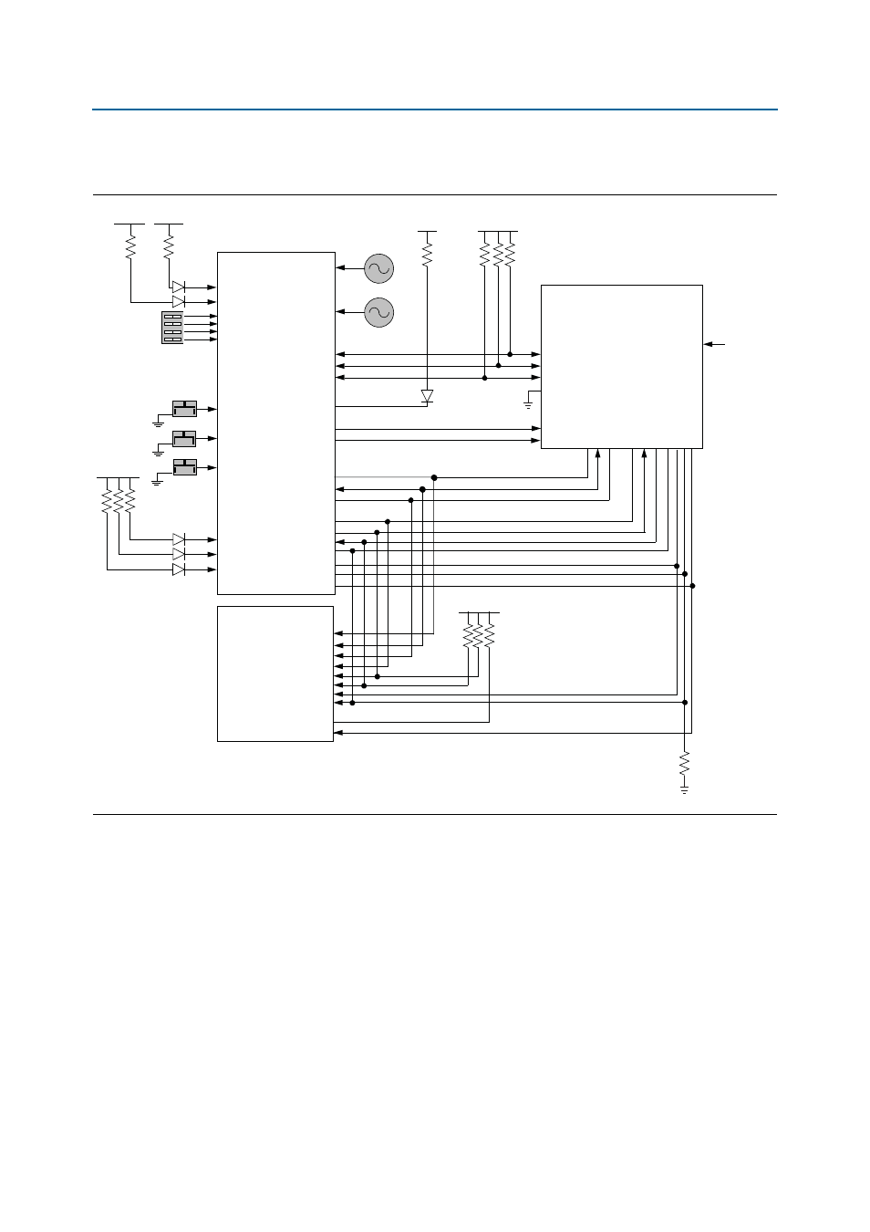
shows the PFL configuration.
f
For more information on the following topics, refer to the respective documents:
■
Board Update Portal, PFL design, and flash memory map storage, refer to the
.
■
PFL megafunction, refer to
FPGA Programming over External USB-Blaster
The JTAG chain header provides another method for configuring the FPGA using an
external USB-Blaster device with the Quartus II Programmer running on a PC. To
prevent contention between the JTAG masters, the embedded USB-Blaster is
automatically disabled when you connect an external USB-Blaster to the JTAG chain
through the JTAG chain header.
Figure 2–4. PFL Configuration
MAX V CPLD
5M2210 System Controller
Cyclone V FPGA
FPGA_DATA [15:0]
FPGA_DCLK
FLASH_A [25:1]
FLASH_D [31:0]
DATA [15:0]
DCLK
nSTATUS
nCONFIG
CONF_DONE
CONF_DONE
MSEL[4:0]
Connects to the
MAX V CPLD
2.5 V
10 k
Ω
nCE
CFI Flash
FLASH_CEn
FLASH_OEn
FLASH_WEn
FLASH_A [25:1]
FLASH_D [15:0]
FLASH_CEn
FLASH_OEn
FLASH_WEn
FLASH_WPn
FLASH_ADVn
FPGA_nCONFIG
FPGA_CONF_DONE
FLASH_RYBSYn0
FLASH_RYBSYn0
FLASH_RYBSYn1
FPGA_nSTATUS
2.5 V
10 k
Ω
FLASH_ADVn
CONF_DONE_LED
2.5 V
FLASH_CLK
FLASH_CLK
FLASH_RSTn
FLASH_RESETn
FPP Mode
Flash Interface
56.2
Ω
100
Ω
56.2
Ω
56.2
Ω
50 MHz
100 MHz
2.5 V
2.5 V
2.5 V
ERROR
LOAD
SEC_MODE
FACT_LOAD
CLK_EN
CLK_SEL
MAX_RESETn
PGM_CONFIG
PGM_SEL
PGM_LED0
PGM_LED1
PGM_LED2
DIP Switch
10 k
Ω