Pci express leds, Character lcd, Pci express leds –22 – Altera Cyclone V GX FPGA Development Board User Manual
Page 30: Character lcd –22
2–22
Chapter 2: Board Components
General User Input/Output
Cyclone V GX FPGA Development Board
May 2013
Altera Corporation
Reference Manual
PCI Express LEDs
Board references D8 through D10 are PCI Express LEDs for link width indication.
There are no board-specific functions for the PCI Express LEDs. You can configure the
LEDs to display the functions as listed in
. The LEDs are driven by the
Cyclone V GX device.
lists the PCI Express LED schematic signal names and their corresponding
Cyclone V GX device pin numbers.
Character LCD
The development board includes a single 14-pin 0.1" pitch dual-row header that
interfaces to a 2 line × 16 character Lumex character LCD. The character LCD has a
14-pin receptacle that mounts directly to the board's 14-pin header, so it can be easily
removed for access to components under the display. You can also use the header for
debugging or other purposes.
Table 2–19
summarizes the character LCD pin assignments. The signal names and
directions are relative to the Cyclone V GX device.
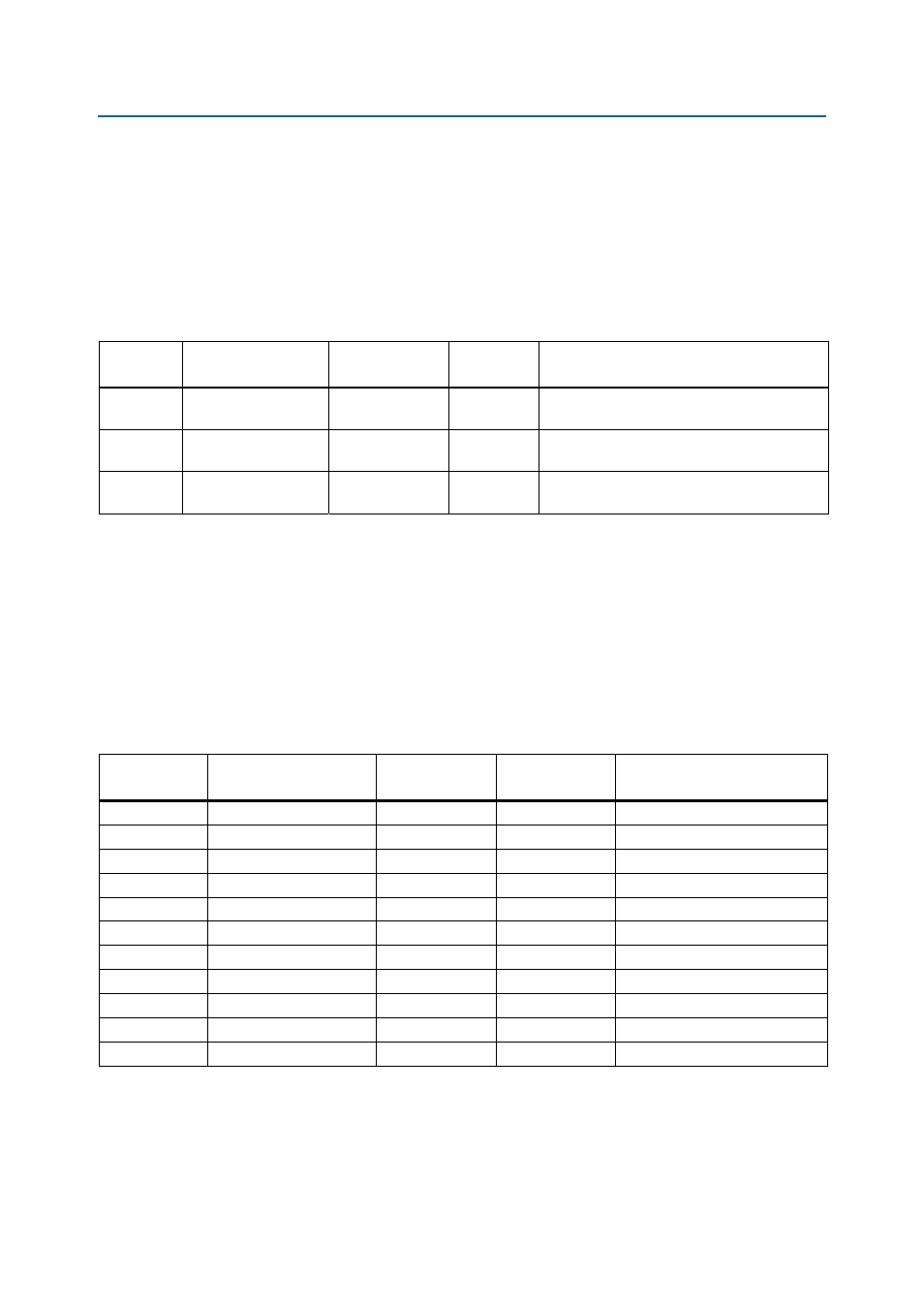
Table 2–18. PCI Express LED Schematic Signal Names and Functions
Board
Reference
Schematic
Signal Name
Cyclone V GX
Pin Number
I/O Standard
Description
D8
PCIE_LED_X1
AD28
2.5-V
Green LED. Configure this LED to display the
PCI Express link width x1.
D9
PCIE_LED_X4
AC29
2.5-V
Green LED. Configure this LED to display the
PCI Express link width x4.
D10
PCIE_LED_G1
AB28
2.5-V
Green LED. Configure this LED to display the
PCI Express Gen1 link.
Table 2–19. Character LCD Pin Assignments, Schematic Signal Names, and Functions
Board
Reference (J18)
Schematic Signal Name
Cyclone V GX
Pin Number
I/O Standard
Description
7
LCD_DATA0
T10
2.5-V
LCD data bus
8
LCD_DATA1
AH5
2.5-V
LCD data bus
9
LCD_DATA2
AH4
2.5-V
LCD data bus
10
LCD_DATA3
U8
2.5-V
LCD data bus
11
LCD_DATA4
T9
2.5-V
LCD data bus
12
LCD_DATA5
AH6
2.5-V
LCD data bus
13
LCD_DATA6
AG6
2.5-V
LCD data bus
14
LCD_DATA7
R12
2.5-V
LCD data bus
4
LCD_D_Cn
D17
2.5-V
LCD data or command select
5
LCD_WEn
E17
2.5-V
LCD write enable
6
LCD_CSn
C11
2.5-V
LCD chip select