Sdi video output/input, Sdi video output/input –31 – Altera Cyclone V GX FPGA Development Board User Manual
Page 39
Chapter 2: Board Components
2–31
Components and Interfaces
May 2013
Altera Corporation
Cyclone V GX FPGA Development Board
Reference Manual
SDI Video Output/Input
The SDI video port consists of a LMH0303 cable driver and a LMH0384 cable
equalizer. The PHY devices from National Semiconductor interface to single-ended
75-
Ω SMB connectors.
The cable driver supports operation at 270 Mbit standard definition (SD), 1.5 Gbit
high definition (HD), and 2.97 Gbit dual-link HD modes. Control signals are allowed
for SD and HD modes selections, as well as device enable. The reference clock of the
device is 148.5 MHz and matches the incoming signals to within 50 ppm using the UP
and DN voltage control lines to the voltage-controlled crystal oscillator (VCXO).
Table 2–25
lists the supported output standards for the SD and HD input.
f
For more information about the application circuit of the cable driver, refer to the
cable driver data sh
133
HSMA_TX_D_N13
C25
LVDS or 2.5-V LVDS TX bit 13n or CMOS bit 62
134
HSMA_RX_D_N13
L19
LVDS or 2.5-V LVDS RX bit 13n or CMOS bit 63
137
HSMA_TX_D_P14
C27
LVDS or 2.5-V LVDS TX bit 14 or CMOS bit 64
138
HSMA_RX_D_P14
G22
LVDS or 2.5-V LVDS RX bit 14 or CMOS bit 65
139
HSMA_TX_D_N14
C26
LVDS or 2.5-V LVDS TX bit 14n or CMOS bit 66
140
HSMA_RX_D_N14
G23
LVDS or 2.5-V LVDS RX bit 14n or CMOS bit 67
143
HSMA_TX_D_P15
B27
LVDS or 2.5-V LVDS TX bit 15 or CMOS bit 68
144
HSMA_RX_D_P15
H21
LVDS or 2.5-V LVDS RX bit 15 or CMOS bit 69
145
HSMA_TX_D_N15
A28
LVDS or 2.5-V LVDS TX bit 15n or CMOS bit 70
146
HSMA_RX_D_N15
G21
LVDS or 2.5-V LVDS RX bit 15n or CMOS bit 71
149
HSMA_TX_D_P16
E26
LVDS or 2.5-V LVDS TX bit 16 or CMOS bit 72
150
HSMA_RX_D_P16
J20
LVDS or 2.5-V LVDS RX bit 16 or CMOS bit 73
151
HSMA_TX_D_N16
E25
LVDS or 2.5-V LVDS TX bit 16n or CMOS bit 74
152
HSMA_RX_D_N16
H20
LVDS or 2.5-V LVDS RX bit 16n or CMOS bit 75
155
HSMA_CLK_OUT_P2
A25
LVDS or 2.5-V LVDS or CMOS clock out 2 or CMOS bit 76
156
HSMA_CLK_IN_P2
L14
LVDS or 2.5-V LVDS or CMOS clock in 2 or CMOS bit 77
157
HSMA_CLK_OUT_N2
A24
LVDS or 2.5-V LVDS or CMOS clock out 2 or CMOS bit 78
158
HSMA_CLK_IN_N2
L13
LVDS or 2.5-V LVDS or CMOS clock in 2 or CMOS bit 79
160
HSMA_PRSNTn
L16
2.5-V CMOS
HSMC port A presence detect
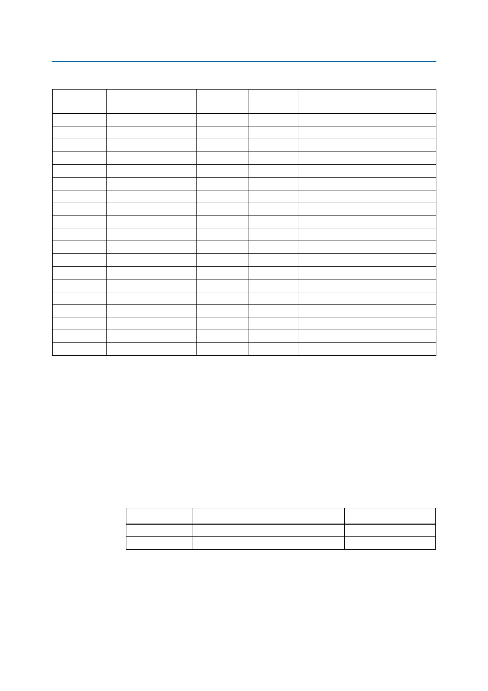
Table 2–24. HSMC Interface Pin Assignments, Schematic Signal Names, and Functions (Part 4 of 4)
Board
Reference (J1)
Schematic Signal Name
Cyclone V GX
Pin Number
I/O Standard
Description
Table 2–25. Supported Output Standards for SD and HD Input
SD_HD Input
Supported Output Standards
Rise TIme
0
SMPTE 424M, SMPTE 292M
Faster
1
SMPTE 259M
Slower