Altera Cyclone II FPGA Starter Development Board User Manual
Page 47
Altera Corporation
Reference Manual
2–29
October 2006
Cyclone II FPGA Starter Development Board
Development Board Components
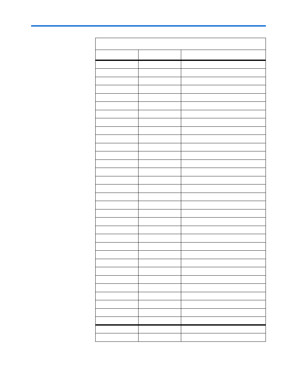
GPIO_0[4]
PIN_A15
GPIO Connection 0[4]
GPIO_0[5]
PIN_B15
GPIO Connection 0[5]
GPIO_0[6]
PIN_A16
GPIO Connection 0[6]
GPIO_0[7]
PIN_B16
GPIO Connection 0[7]
GPIO_0[8]
PIN_A17
GPIO Connection 0[8]
GPIO_0[9]
PIN_B17
GPIO Connection 0[9]
GPIO_0[10]
PIN_A18
GPIO Connection 0[10]
GPIO_0[11]
PIN_B18
GPIO Connection 0[11]
GPIO_0[12]
PIN_A19
GPIO Connection 0[12]
GPIO_0[13]
PIN_B19
GPIO Connection 0[13]
GPIO_0[14]
PIN_A20
GPIO Connection 0[14]
GPIO_0[15]
PIN_B20
GPIO Connection 0[15]
GPIO_0[16]
PIN_C21
GPIO Connection 0[16]
GPIO_0[17]
PIN_C22
GPIO Connection 0[17]
GPIO_0[18]
PIN_D21
GPIO Connection 0[18]
GPIO_0[19]
PIN_D22
GPIO Connection 0[19]
GPIO_0[20]
PIN_E21
GPIO Connection 0[20]
GPIO_0[21]
PIN_E22
GPIO Connection 0[21]
GPIO_0[22]
PIN_F21
GPIO Connection 0[22]
GPIO_0[23]
PIN_F22
GPIO Connection 0[23]
GPIO_0[24]
PIN_G21
GPIO Connection 0[24]
GPIO_0[25]
PIN_G22
GPIO Connection 0[25]
GPIO_0[26]
PIN_J21
GPIO Connection 0[26]
GPIO_0[27]
PIN_J22
GPIO Connection 0[27]
GPIO_0[28]
PIN_K21
GPIO Connection 0[28]
GPIO_0[29]
PIN_K22
GPIO Connection 0[29]
GPIO_0[30]
PIN_J19
GPIO Connection 0[30]
GPIO_0[31]
PIN_J20
GPIO Connection 0[31]
GPIO_0[32]
PIN_J18
GPIO Connection 0[32]
GPIO_0[33]
PIN_K20
GPIO Connection 0[33]
GPIO_0[34]
PIN_L19
GPIO Connection 0[34]
GPIO_0[35]
PIN_L18
GPIO Connection 0[35]
GPIO_1[0]
PIN_H12
GPIO Connection 1[0]
GPIO_1[1]
PIN_H13
GPIO Connection 1[1]
Table 2–14. Expansion Header FPGA Pin Connections (Part 2 of 3)
Signal Name
FPGA Pin
Description