Clock circuit, Clock circuit schematic, Clock circuit –13 – Altera Cyclone II FPGA Starter Development Board User Manual
Page 31
Altera Corporation
Reference Manual
2–13
October 2006
Cyclone II FPGA Starter Development Board
Development Board Components
Clock Circuit
The development board has four clock sources:
■
Two on-board oscillators produce 27 MHz and 50 MHz clock signals.
■
A SubMiniature version A (SMA) connector, EXT CLK, located near
the right bottom corner of the board enables an external clock source
to provide clocking.
■
Input through the USB-Blaster port can provide a 24 MHz clock.
Clock Circuit Schematic
shows the clock circuit schematic.
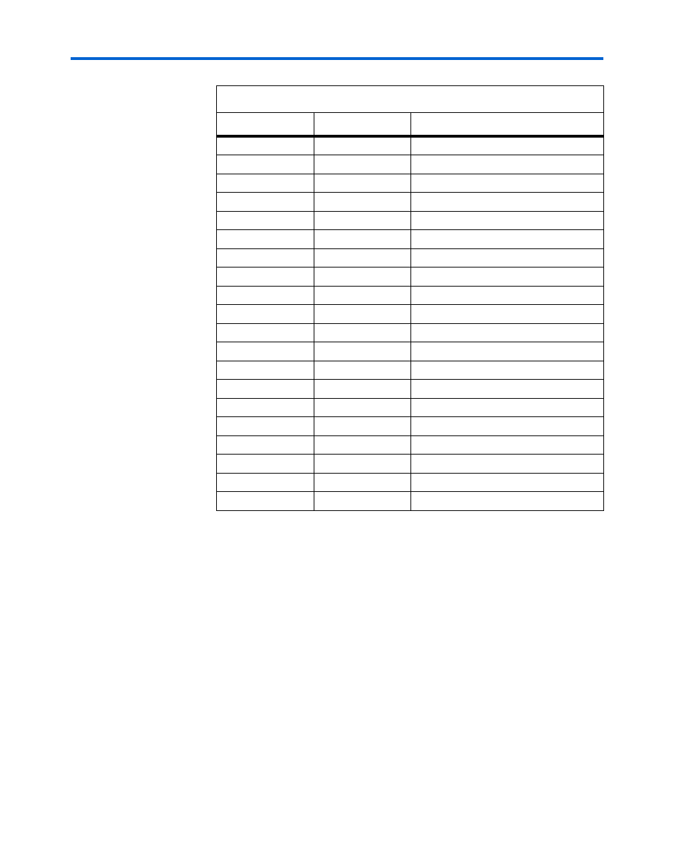
FL_ADDR[15]
PIN_AA12
FLASH Address[15]
FL_ADDR[16]
PIN_AB12
FLASH Address[16]
FL_ADDR[17]
PIN_AA20
FLASH Address[17]
FL_ADDR[18]
PIN_U14
FLASH Address[18]
FL_ADDR[19]
PIN_V14
FLASH Address[19]
FL_ADDR[20]
PIN_U13
FLASH Address[20]
FL_ADDR[21]
PIN_R13
FLASH Address[21]
FL_ADDR[0]
PIN_AB20
FLASH Address[0]
FL_ADDR[1]
PIN_AA14
FLASH Address[1]
FL_DQ[0]
PIN_AB16
FLASH Data[0]
FL_DQ[1]
PIN_AA16
FLASH Data[1]
FL_DQ[2]
PIN_AB17
FLASH Data[2]
FL_DQ[3]
PIN_AA17
FLASH Data[3]
FL_DQ[4]
PIN_AB18
FLASH Data[4]
FL_DQ[5]
PIN_AA18
FLASH Data[5]
FL_DQ[6]
PIN_AB19
FLASH Data[6]
FL_DQ[7]
PIN_AA19
FLASH Data[7]
FL_OE_N
PIN_AA15
FLASH Output Enable
FL_RST_N
PIN_W14
FLASH Reset
FL_WE_N
PIN_Y14
FLASH Write Enable
Table 2–8. Flash Memory FPGA Pin Connections (Part 2 of 2)
Signal Name
FPGA Pin
Description