Altera I/O Buffer (ALTIOBUF) IP Core User Manual
Page 2
buffers, you can connect these ports to the ALTOCT IP core to enable dynamic calibration for on-chip
termination.
The additional dynamic termination control ports allow control when series termination or parallel
termination are enabled for bidirectional buffers. Parallel termination needs to only be enabled when the
bidirectional I/O is receiving input. Otherwise, it needs to be disabled so that the output performance and
power dissipation is optimal.
Another key application for this IP core is for dynamic delay chain in the I/O buffer. Dynamic I/O delay
allows implementing automatic deskew, especially for memory interfaces, such as DDR3, which is
handled by the memory interface intellectual property (IP). You need to dynamically deskew and not
calculate manually because much of the skew can come from the I/O buffers of either the FPGA or the
other device the FPGA is interfacing with (for example, memory). Even if the trace lengths are matched,
there can still be electrical skew in the system. Also, this skew changes and can change from device to
device. Having the ability to deskew from the fabric allows you to remove uncertainties that would have to
be considered in the timing budget. This allows you to gain more timing margin, which allows higher
frequencies.
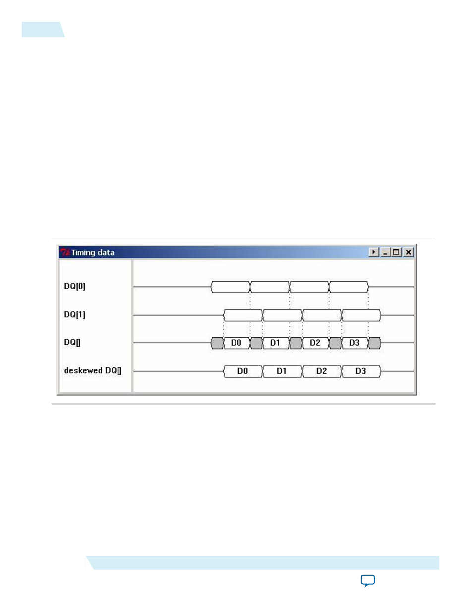
Figure 1: Example Illustrating Deskew
This figure shows an example of deskew.
For example, if the input (or output) bus signals are
DQ[0]
and
DQ[1]
, board trace skew, transmitter
device skew, or even FPGA package skew could cause signals that were initially aligned to become
misaligned. The third waveform shows the window available to the receiver for capturing the data. If
DQ[0]
was delayed a bit to match
DQ[1]
, a wider window would become available to the receiver.
Note: The deskew delay chains are not meant to find the middle of a data valid window, but just to
deskew the incoming (or outgoing) data to widen the overall window for a bus of inputs (or
outputs). To do this, you only need to align just one edge (for example, the left edge) of the data
valid window of all the pins.
To find the left and right edges of the data valid window, you need to do coarser adjustments (one
possible method is to use the new phase adjustment functionality of the PLL (ALTPLL IP core). The range
2
ALTIOBUF Common Application
UG-01024
2014.12.15
Altera Corporation
I/O Buffer (ALTIOBUF) IP Core User Guide