Altiobuf references, Altiobuf signals and parameters: as input buffer – Altera I/O Buffer (ALTIOBUF) IP Core User Manual
Page 16
ALTIOBUF References
Provides the signals, parameters, Verilog HDL prototype, and VHDL component declaration for
ALTIOBUF IP core.
Related Information
Using the Port and Parameter Definitions
ALTIOBUF Signals and Parameters: As Input Buffer
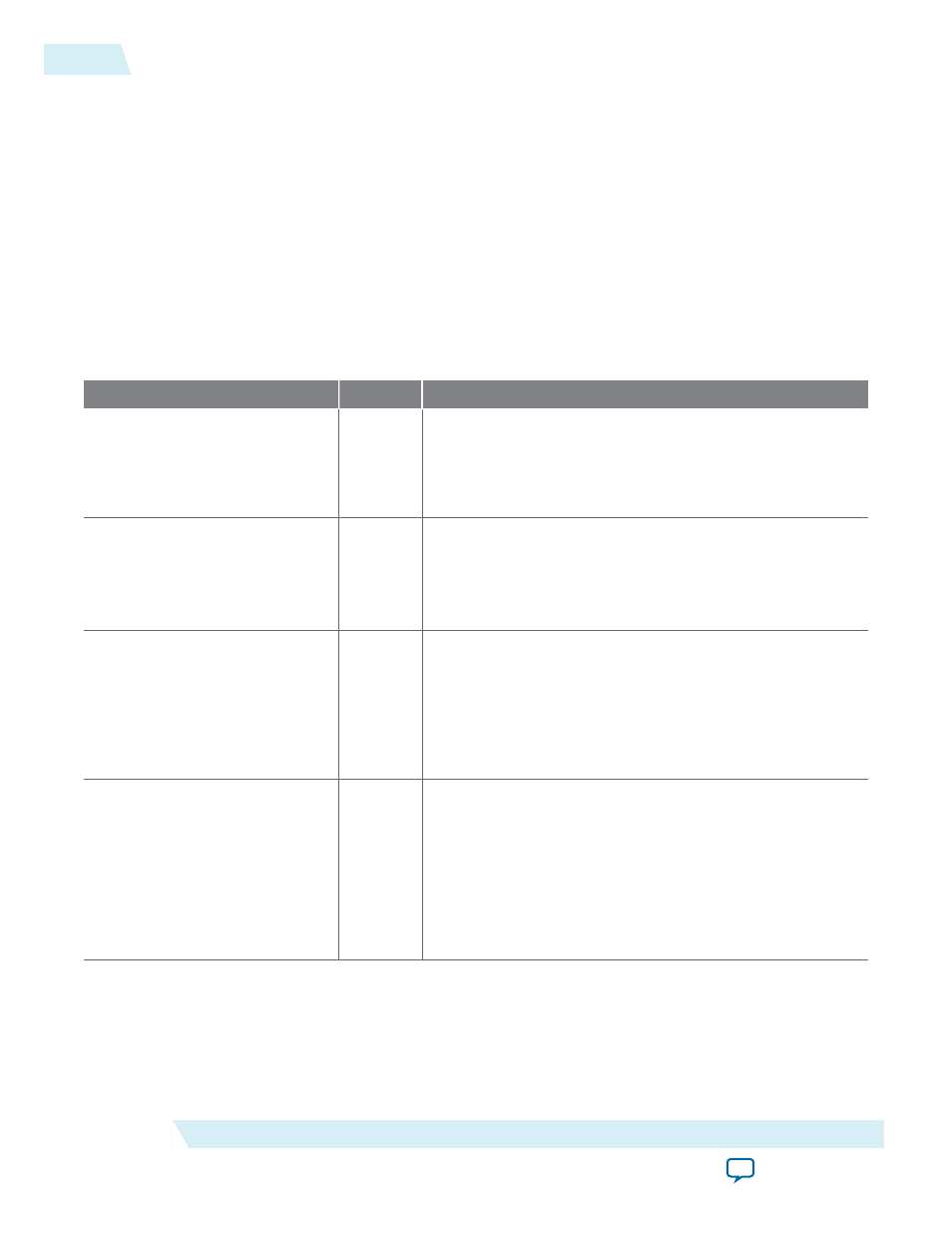
Table 6: ALTIOBUF (As Input Buffer) Input Ports
This table lists the input ports for the ALTIOBUF IP core (as input buffer).
Name
Required
Description
datain[]
Yes
The input buffer normal data input port.
Input port
[NUMBER_OF_CHANNELS - 1..0]
wide. The
input signal to the I/O output buffer element. For differen‐
tial signals, this port acquires the positive signal input.
datain_b[]
No
The negative signal input of a differential signal to the I/O
input buffer element. Input port
[NUMBER_OF_CHANNELS -
1..0]
wide. When connected, the
datain_b
port is always
fed by a pad/port atom. This port is used only if the
USE_
DIFFERENTIAL_MODE
parameter value is
TRUE.
io_config_datain
No
Input port that feeds the datain port of
IO_CONFIG
for user-
driven dynamic delay chain.
Input port used to feed input data to the serial load shift
register. The value is a 1-bit wire shared among all I/O
instances. This port is available only if the
USE_IN_
DYNAMIC_DELAY_CHAIN
parameter value is
TRUE
.
io_config_clk
No
Input clock port that feeds the
IO_CONFIG
for user-driven
dynamic delay chain. Input port used as the clock signal of
shift register block.
The maximum frequency for this clock is 30 MHz.
The value is a 1-bit wire shared among all I/O instances.
This port is available only if the
USE_IN_DYNAMIC_DELAY_
CHAIN
parameter value is
TRUE.
16
ALTIOBUF References
UG-01024
2014.12.15
Altera Corporation
I/O Buffer (ALTIOBUF) IP Core User Guide