Altiobuf input, output, and oe paths, Altiobuf input buffer – Altera I/O Buffer (ALTIOBUF) IP Core User Manual
Page 11
ALTIOBUF Input, Output, and OE Paths
The three path types used with the I/O buffer in the delay chain architecture are input path, output path,
and oe path.
Dynamic delay chains are integrated in the input path for input and bidirectional buffers. Dynamic delay
chains are integrated in the output and oe paths for output and bidirectional buffers. This section
describes the dynamic delay chain-related components only.
All paths share a similar configuration in which the delay cells are getting their delay control signal from
the IO_CONFIG component. For the input path, the IO_CONFIG’s
PADTOINPUTREGISTERDELAYSETTING
output port drives the DELAY_CHAIN’s (input delay cell)
DELAYCTRLIN
input port. For the output and
oe path, use the IO_CONFIG’s
OUTPUTDELAYSETTING
1 and 2 output ports to drive the
DELAYCTRLIN
port
of the first and second output delay cells, respectively.
The number of delay chains needed is
NUMBER_OF_CHANNELS
. Each instance of the I/O buffer includes a
delay chain. Assume
NUMBER_OF_CHANNELS
is equal to ×. There must be × instances of input delay chain
for × input buffer, and 2× instances of the first output delay chain and 2× instances of the second output
delay chain output buffer because it uses the output and oe paths. The bidirectional buffer combines all
instances of the delay chains mentioned above.
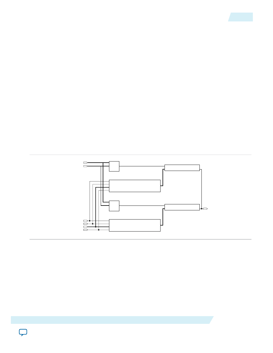
Figure 6: Sample ALTIOBUF (Input Buffer Mode) Architecture when NUMBER_OF_CHANNELS = 2
This figure shows the internal architecture of the ALTIOBUF IP core (input buffer mode) when
NUMBER_OF_CHANNELS is equal to 2 and the dynamic delay chain feature is enabled.
STRATIXIII_DELAY_CHAIN
STRATIXIII_DELAY_CHAIN
dataout[1..0]
input_dyn_delay_chaina_1
DATAIN
DELAYCTRLIN[3..0]
DATAOUT
input_dyn_delay_chaina_0
DATAIN
DELAYCTRLIN[3..0]
DATAOUT
STRATIXIII_IO_IBUF
ibufa_1
I
IBAR O
ioconfiga_1
STRATIXIII_IO_CONFIG
DATAIN
CLK
ENA
PADTOINPUTREGISTERDELAYSETTING[3..0]
UPDATE
io_config_datain
io_config_clk
io_config_clkena[1..0]
io_config_update
datain[1..0]
datain_b[1..0]
STRATIXIII_IO_IBUF
ibufa_0
I
IBAR O
ioconfiga_0
STRATIXIII_IO_CONFIG
DATAIN
CLK
ENA
PADTOINPUTREGISTERDELAYSETTING[3..0]
UPDATE
ALTIOBUF Input Buffer
The input buffer IP core uses the input path of the dynamic delay chain.
The
datain
and
datain_b
input ports of the ALTIOBUF IP core (input buffer mode) connect to the
i
and
ibar
ports (if differential mode is enabled) of the input buffer, respectively. In the input path, the
value of the input buffer’s
dataout
port is passed into the input delay chain. The
dataout
port of the
ALTIOBUF IP core (input buffer mode) is the output of the
dataout
delay chain.
You must add a register external to the IP core, either a regular DFFE or a DDIO and connect its input to
the IP core’s
dataout
port.
UG-01024
2014.12.15
ALTIOBUF Input, Output, and OE Paths
11
I/O Buffer (ALTIOBUF) IP Core User Guide
Altera Corporation