Output path waveform, Oe path, Interfaces – Altera GPIO User Manual
Page 8
Output Path Waveform
The waveform for the output path is similar to
.
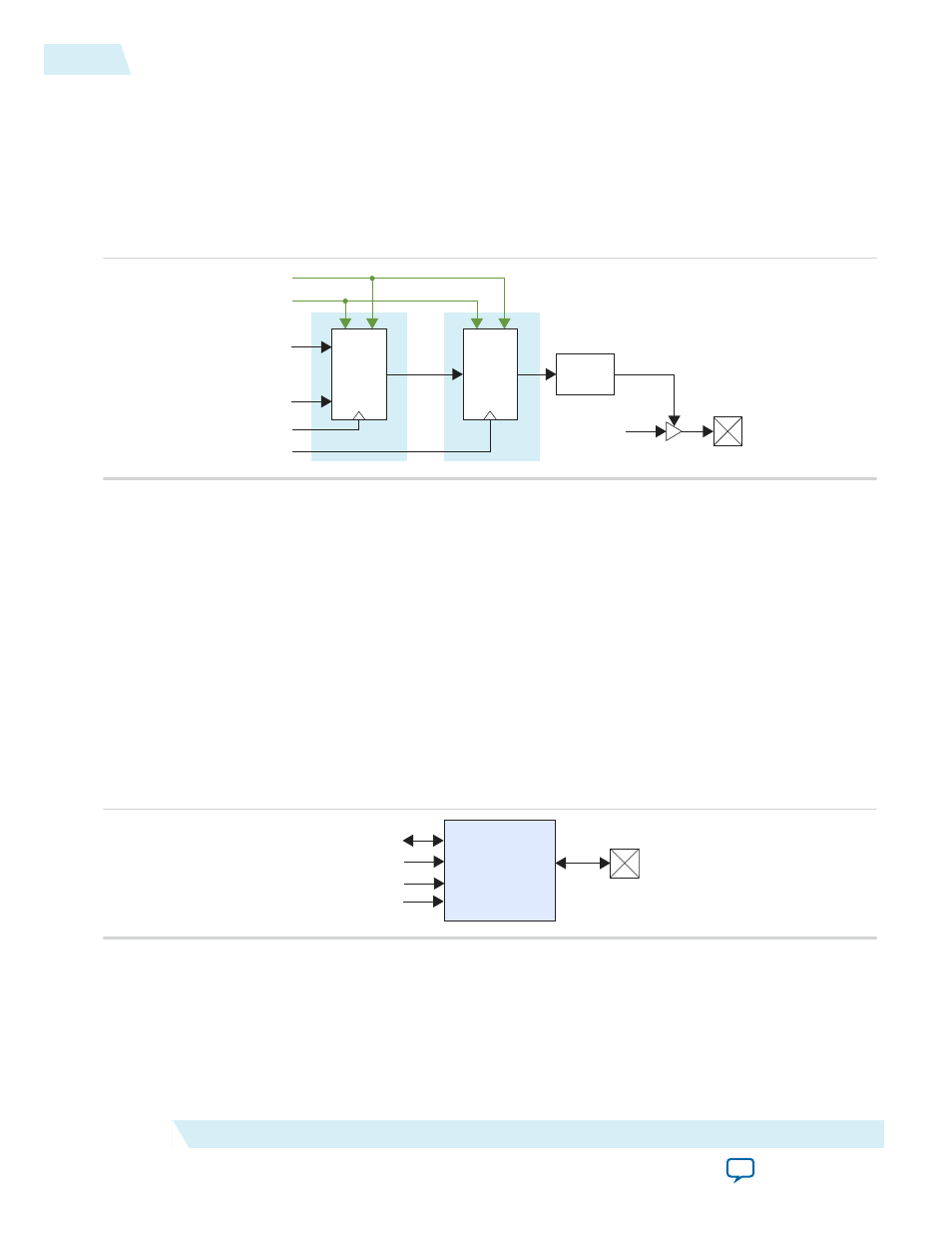
OE Path
The following figure shows the simplified view of a GPIO OE path.
Figure 5: OE Path (Simplified View)
ACLR_N
APRE_N
OEIN[0]
OEIN[1]
CLK_HR
CLK_FR
DDIO
OUT
FF
Delay
Element
HR
FR
From Output
Data Path
The simplified view of a GPIO OE path is similar to the
. The difference between output path and
OE path is that the OE path does not support full-rate DDIO mode. Therefore, there is no full-rate DDIO
in OE path. To support packed-register implementations in the OE path, a simple register operates as full-
rate DDIO. For the same reason, there is no need for two half-rate DDIOs. Only one is present.
The OE path operates in the following three fundamental modes:
• Bypass—the core sends data directly to the delay element, bypassing all DDIOs.
• Packed Register—bypasses half-rate DDIO.
• SDR output, half-rate—half-rate DDIOs convert data from full-rate to half-rate.
Interfaces
The following figure shows the main interfaces for the Altera GPIO IP core.
Figure 6: Altera GPIO IP Core Interfaces Diagram
Pad
Data
Clock
Altera GPIO
Termination
Reset
8
Output Path Waveform
ug-altera_gpio
2014.08.18
Altera Corporation
Altera GPIO IP Core User Guide