Register packing, Altera gpio timing – Altera GPIO User Manual
Page 14
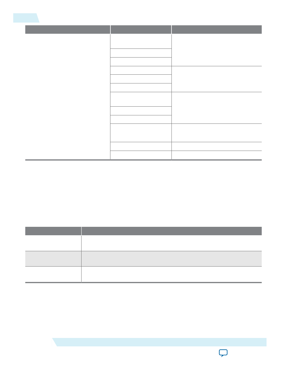
Signal Name
Configuration
Clock
sclr
/
sset
/ all pad signals
Register Mode: Simple
Register/DDIO
ck
Half rate: not used
Separate Clocks: off
Register Mode: DDIO
ck_fr
Half rate: used
Separate Clocks: off
Register Mode: Simple
Register/DDIO
• Input path: ck_in
• Output path: ck_out
Half rate: not used
Separate Clocks: on
Register Mode: DDIO
• Input path: ck_fr_in
• Output path: ck_fr_out
Half rate: used
Separate Clocks: on
Register Packing
The Altera GPIO IP core allows you to pack register into the periphery to save area and resource utiliza‐
tion.
You can configure the full-rate DDIO on the input and output path as a flip flop. To do so, add the .qsf
assignments listed in this table.
Table 4: Register Packing QSF Assignments
Path
QSF Assignment
Input register packing
set_instance_assignment -name FAST_INPUT_REGISTER ON -to register> Output register packing set_instance_assignment -name FAST_OUTPUT_REGISTER ON -to register> Output enable register packing set_instance_assignment -name FAST_OUTPUT_ENABLE_REGISTER ON -to Note: These assignments do not guarantee register packing but rather enable the Fitter to find a legal placement. Otherwise, the Fitter will keep the flip flop in the core. Altera GPIO Timing The Quartus II software version 14.0a10 does not automatically generate the timing constraints. 14 Register Packing ug-altera_gpio 2014.08.18 Altera Corporation Altera GPIO IP Core User Guide