Mechanical parts, What are they, Printed circuit boards – Elenco Electronic Component Kit User Manual
Page 22: Design rules
-21-
MECHANICAL PARTS
PRINTED CIRCUIT BOARDS,
What are they?
A printed circuit is a conductive pattern glued to one
or both sides of an insulating material. Holes are
punched or drilled through the conductor and board
to allow the interconnection of electronic parts. In
the case of a double sided board, the holes are
plated to provide a connection between the
conductors on both sides of the board. This method
provides considerable space savings over hand
wiring and allows for automated insertion and
soldering of parts. A more uniform product is
produced because wiring errors are eliminated. The
insulating material thickness may vary from 0.015”
to 0.500”. The most widely used base material is
NEMA-XXXP paper base phenolic. Copper is the
most common conductive material glued to the
base. The common thicknesses of the copper foil
are 0.0014” (1 oz./sq. ft.) and 0.0028” (2 oz./sq. ft.).
For single sided boards, the copper is laminated to
the board and then screened and etched away.
Double sided boards use a plating process and
conductive ink to achieve the desired layout.
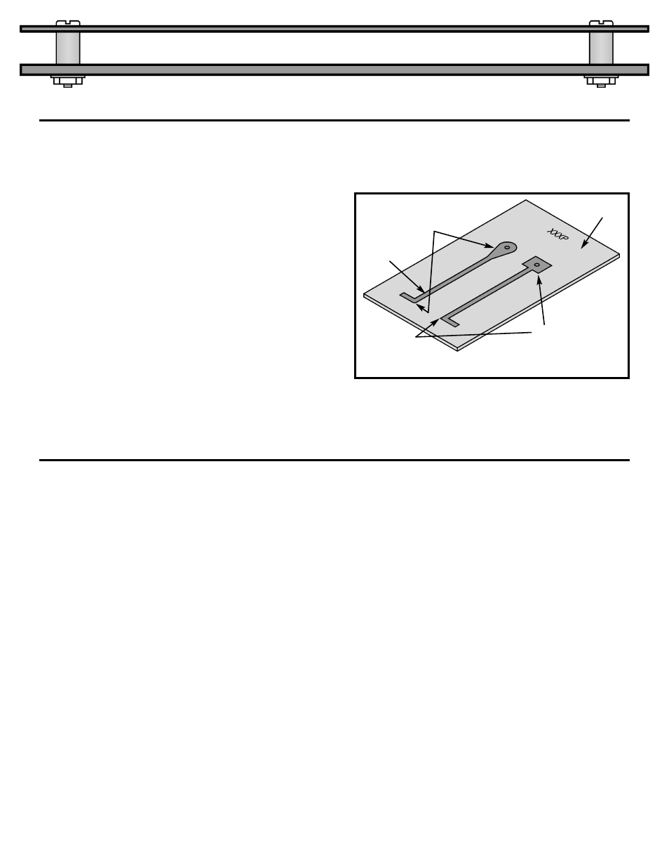
Figure 34
Insulating
Material
Wrong
Copper
Correct
DESIGN RULES
After a the breadboard has been tested, there are
some design rules used to layout the printed circuit
board. A few of these basic rules are listed here:
1. Diameter of punched holes should not be less
than 2/3 the board thickness.
2. Distance between punched holes or between
holes and board edge should not be less than the
board thickness.
3. Holes should not exceed more than 0.020” of the
diameter of the wire to be inserted in the hole
(machine insertion may require more, but leads
should be “clinched”).
4. Conductor widths should be large enough to
carry current peaks. A width of one tenth of an
inch (1 oz./sq. ft. copper) will increase in
temperature 10
O
C at a DC current of 5A.
5. Conductor spacing must be capable of
withstanding applied voltages. If a voltage
difference of 500 volts exists between two copper
runs, they must be separated by at leads 0.03” to
prevent breakdown.
6. Avoid the use of sharp corners when laying out
copper (see Figure 34). Sharp corners produce
high electric fields that can lower breakdown.
Sharp corners will also make it easier for copper
to peel from the board.
7. Heavy parts must be mounted to prevent board
damage if the unit is dropped.
8. The printed circuit board must be fastened to
prevent leads from touching the case or any other
object mounted near the board.
9. Mounting hardware must be designed to prevent
board stress (warping or excessive torque).